To learn how computers work it is helpful to build a simple computer. This 4-bit computer is built on 32 breadboards and uses 962 NPN BJT transistors. It is powered by a 5-volt rechargeable battery pack and uses about 1 AMP of current. Other components used include resistors LEDs, capacitors, and 22 gauge wires. It is awesome that a functional computer can be built using only these discrete electrical components.
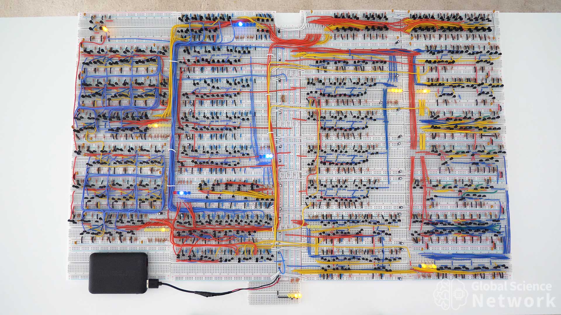
The photo above shows the completed computer. When operating the computer can add or subtract values up to 15. It can hold seven operational commands and store three values to load A, add, or subtract.
The video above describes exactly how the full computer works. I would highly recommend watching the entire video.
When the computer was about half finished I made the video above. The computer is actually functional however the registeres, databus, and ALU signals need to be controlled manually. This is actually a very helpful way to show exactly how information is being sent around the computer and performing mathematical operations.
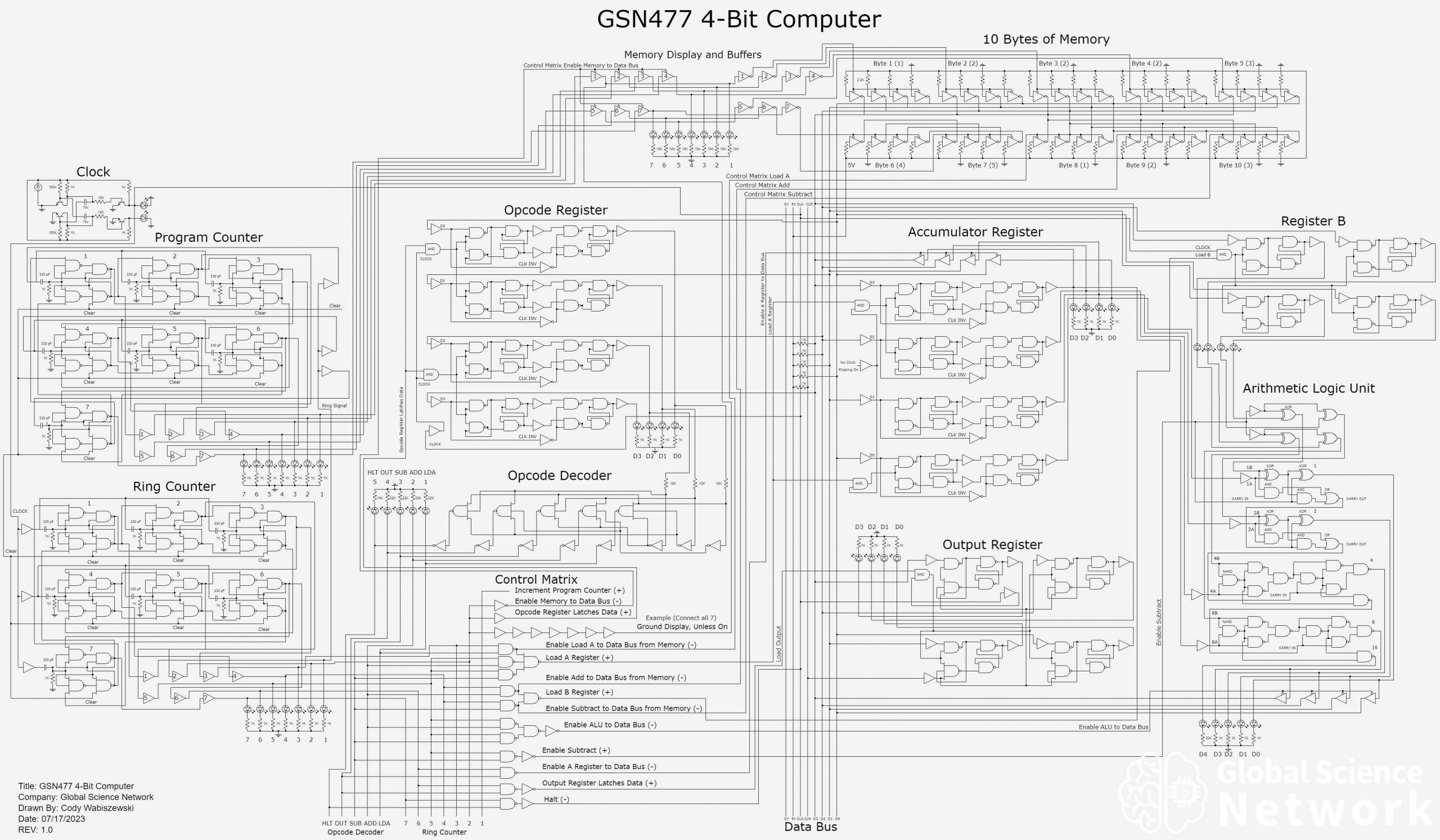
A complete logic gate-level circuit diagram of the 4-bit computer is shown above. Sections of the computer include the clock, program counter, ring counter, opcode register, opcode decoder, control matrix, data bus, 10 bytes of 4-bit memory, accumulator register, output register, register B, and the arithmetic logic unit which is also called the ALU.
Computer Clock
The computer clock is built with an a-stable multi-vibrator. This circuit produces an even square wave where the output signal is either on or off. It is built with four transistors and two 10 microfard capacitors. In the video, the clock is completing a full cycle once every 1.75 seconds. The clock rate can be increased significantly higher than this but to see how the computer works this is a good clock rate.
Program Counter
In most computers, the program counter is a binary counter which is shown in the video below. For the 4-bit computer, it was easier to have the program counter be a 7-stage ring counter. This is because if a binary counter was used the memory module would have had to decode the binary number into individual signals. The ring counter already has the individual signals as the default output.
Ring Counter
The 7-stage ring counter was built with four edge-triggered data flip flops. Each trigger is built with a 330 picofarad capacitor and a 1K resistor. Each time the clock completes one full cycle the ring counter increments. The output of the ring counter goes to the control matrix and enables when information will be sent to different parts of the computer.
Opcode Register
Information is sent from the memory module into the opcode register where this value gets latched. Once the data is latched it is continuously being sent into the opcode decoder. The opcode register gets enabled from a control signal coming from the control matrix.
Opcode Decoder
A binary value is continuously being sent from the opcode register into the opcode decoder. Using inverters and multiple input NAND gates the opcode decoder turns the binary value into a single on output which represents load A, add, subtract, output, and halt commands. These commands get sent into the control matrix to control when circuits in the computer are enabled.
Control Matrix
Signals from the ring counter and opcode decoder are sent to the control matrix. Depending on the values of these signals will determine the output of the control matrix. Circuits in the control matrix are inverters or multiple input NAND gates.
Data Bus
The data bus allows signals to be connected from one circuit to another. Only one circuit should be sending data to the data bus at one time. By default, the data bus has all the data lines on. This is because pull-up resistors are connected from positive 5-volts to each data line. When a circuit connects to the data bus it actually just grounds the data lines that should be off. This makes it so the proper value is on the data bus. When no circuits are connected to the data bus all the data lines are on. There are four other lines of the data bus which include ground, positive 5 volts, the clock signal, and clear. When the clear line is connected to ground it sets the counters to 1 and the output register to zero.
10 Bytes of 4-Bit Memory
The memory module consists of the memory display with buffers and 10 bytes of memory. When memory is being sent to the data bus the display will show which byte is being sent. Each byte of memory is hard coded based on whether resistors are connected to positive or ground. If the resistor is connected to the ground it is on and it if is connected to 5 volts it is off. This is because each byte is connected to the data bus via simplified tri-site buffers which invert the value. The first seven bytes of memory store the opcode instructions, byte 8 contains the load A value, byte 9 is the add value, and byte 10 holds the subtract value.
Accumulator Register
Data is sent to the accumulator register via the data bus. These values get latched in the master-slave data flip-flop and are continuously being sent into the ALU. During the 5 and 6 stages of the ring counter cycle, the value for the ALU will be sent to the data bus and latched into the accumulator register. This makes it so the value the ALU computes can be used in the next ring counter cycle.
Output Register
The output register is made with four regular data flip-flops. When the entire program is complete the final value gets latched into the output register. How this computer is built the output is displayed on LEDs but does not get sent to other circuits.
Register B
Data gets sent from the memory module to the data bus to get latched in register B. Once the value gets latched it is continuously being sent into the ALU. Each bit value gets latched into a regular data flip-flop. This register is built very similarly to register B.
Arithmetic Logic Unit, ALU
The ALU allows the computer to add and subtract numbers up to 15. This is done by using four full adders and four XOR subtract gates. Data is sent into the ALU from the accumulator register and register B. The output is displayed on LEDs and is sent to the data bus via tri-state buffers.
Most people are familiar with the base 10 number system. Computers operate using the base two number system which is also called binary. The video above shows how computers add numbers by using a 4-bit calculator I built on breadboards. If you watch this you will have a good understanding of how the ALU of the computer works.
This video shows how to build a 4-bit calculator using individual transistors. Four full adders are built to be able to add numbers up to 31 as the output has 5-bits.
Final Thoughts
Building a transistor computer on breadboards helps explain how a computer works. It also helps teach logic gate circuit design, data flip-flop design, and how to build each circuit of the computer. If I tried to build the processor in my current personal computer which has about 3 billion transistors it would take about 100 million breadboards to build. This computer also has 32 GB of RAM which has around 35 billion transistors, the 8GB NVIDIA GPU has around 7 billion transistors, and the 1 TB SSD has around 3 trillion transistors. So clearly this could not be built on breadboards.
However, when computers were first being built they were much larger than this breadboard computer. As technology progressed transistors and computers were able to be built much smaller. My next goal is to build artificial neurons. At first, they will be large and bulky but eventually, we should be able to build billions of neurons and trillions of synapses on a very small silicon or carbon substrate.
Cody started the Global Science Network with the idea people should be focusing more time, energy, and resources on useful projects. He has a bachelor’s degree in aerospace engineering and a master’s degree in mechanical engineering. Cody has worked for the US federal government, a university, a large corporation, small businesses, and for himself. He has done human brain computer interface research and is currently working towards creating non-biological human consciousness.