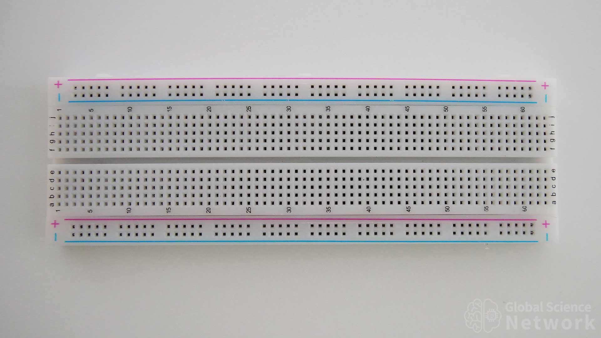
A full adder uses multiple logic gates to add inputs A, B, and carry in. It has two outputs which are the carry-out bit and the sum bit. By sending the carry-out bit to the carry-in of the next full adder an extra bit is added to the output. This means that a larger number can be summed. For example, a single full adder can only add to 11 in binary which is three. When two full adders are wired together the output can be 111 which is seven.
Full Adder 1 Built With XOR, AND, and OR Logic Gates
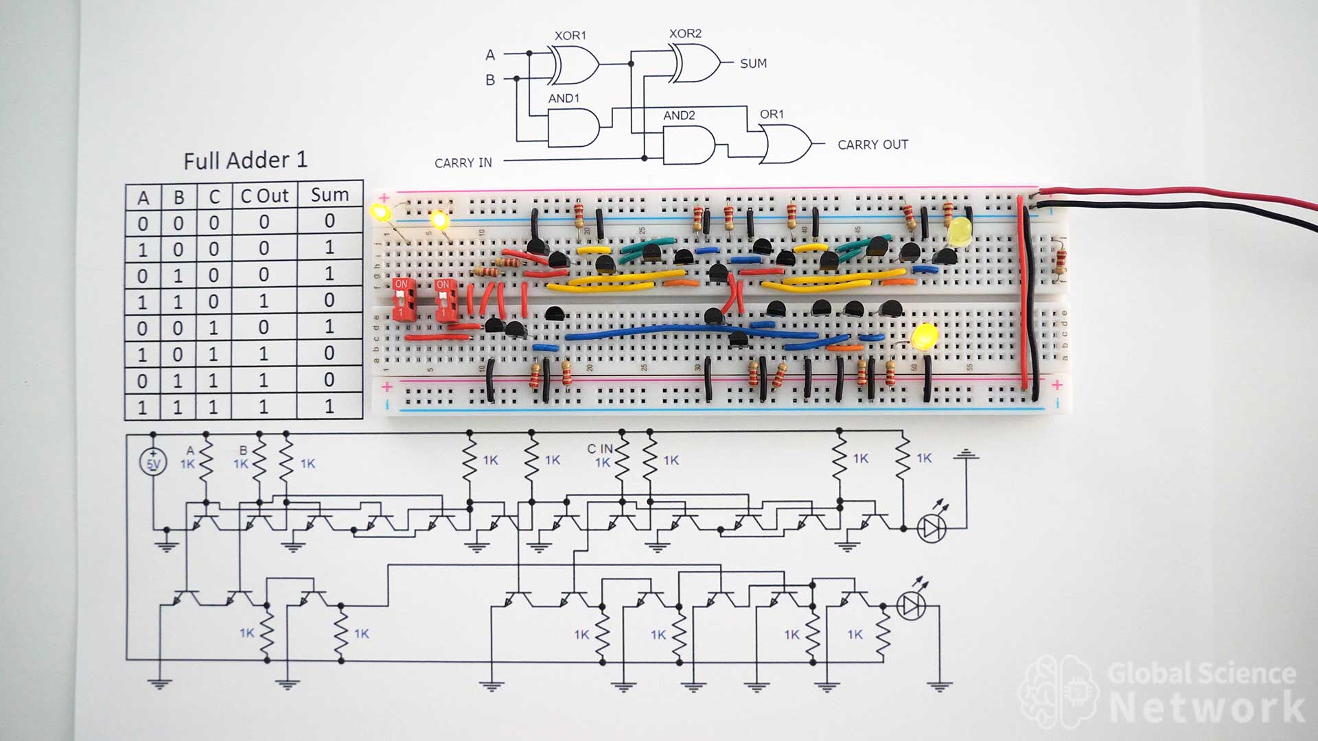
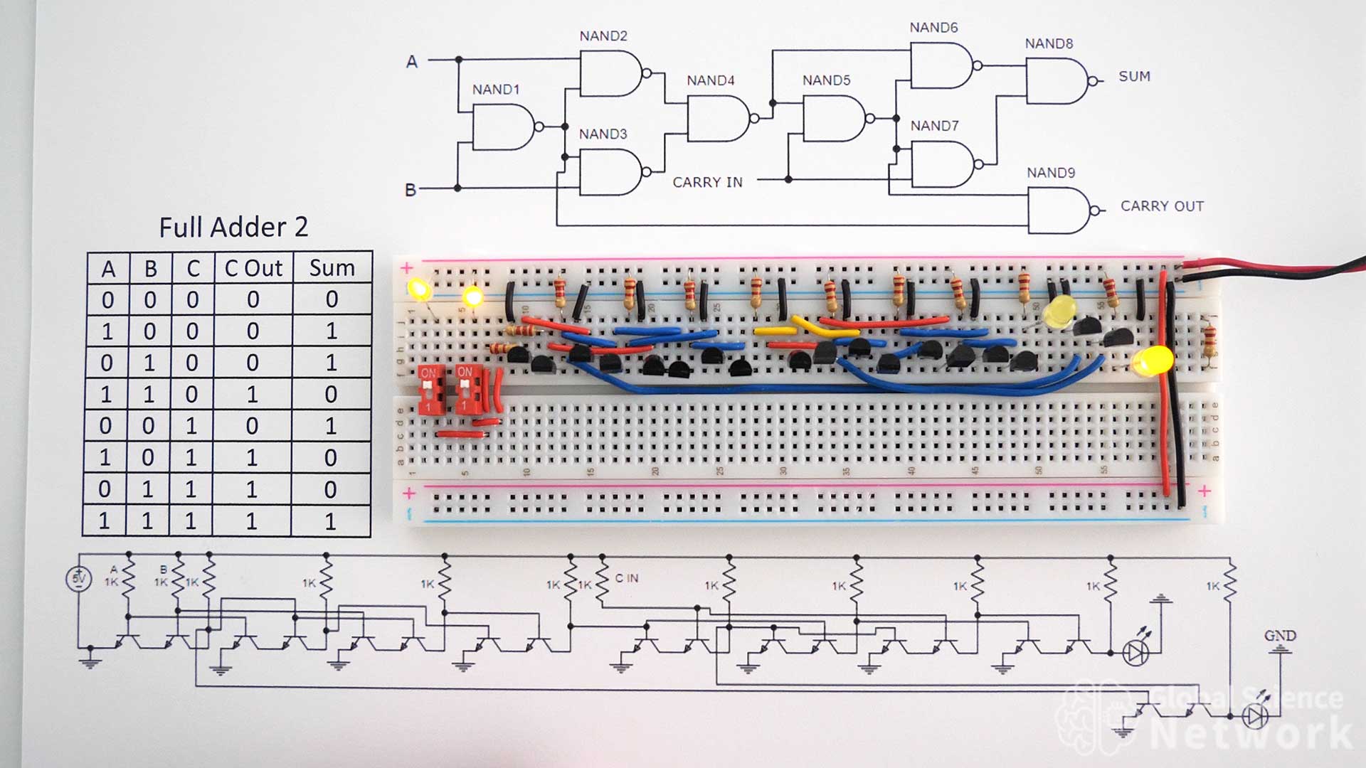
The photo above shows a full adder that I built on a breadboard using individual transistors. There are a total of 5 logic gates used to build the full adder. The logic gates used are two XOR gates, two AND gates, and an OR gate. This took 21 transistors to build. Inputs A and B come from the positive 5-volt rail on the upper left side of the breadboard. The inputs are turned on and off by using two dip switches. The two LEDs in the upper left corner represent inputs A and B. While the two LEDs on the right side of the breadboard represent the two output bits. The resistor values used are all 2.2K.
The circuit in the photo has inputs A and B on and the carry-in off. This makes the carry-out on and the sum bit off which makes the output value 10 in binary which is two. The adder case is therefore 1 + 1 + 0 equals 10.
On the upper half of the breadboard, the two XOR gates are built. The first 6 transistors are the first XOR gate and the second 6 transistors are the second XOR gate. On the bottom half of the breadboard are the two AND gates and the OR gate. The first three transistors are the first AND gate, the next three transistors are the second AND gate and the final three transistors are the OR gate. Different color wires are placed to make each connection type clear. Black jumper wires are always used to connect to the ground.
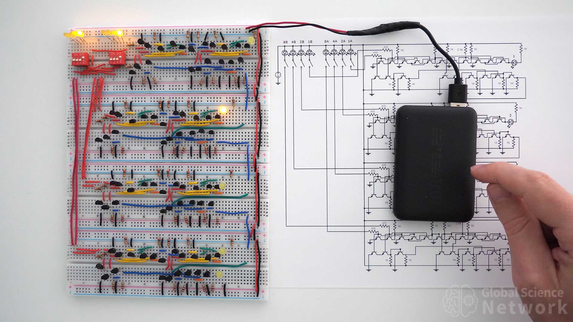
In the video above I show the 4 different ways to build a full adder. I start by showing how to build a half-adder which is more simple but not nearly as useful. The best way to build a full adder will depend on the requirements. It may be best to use all the same type of logic gate, or it might be best to use the least number of transistors.
Full Adder Truth Table
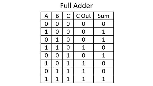
The truth table for a full adder is shown above. Even though I will show four different ways to build a full adder the truth table is always the same. The truth table shows the value of the output bits carry out and sum based on the input bits A, B, and Carry in. If all the inputs are off the outputs are off. When only one input is on only the sum bit is on. If two inputs are on then only the carry-out bit will be on. Finally when all three inputs are on the carry-out bit and sum bit will be on.
The inputs can equal zero or 1. Outputs are binary values that are based on the base 2 number system. When the sum bit is on it represents a value of 1 and when the carry-out bit is on it has a value of 2. So outputs of 00 equal 0, 01 equal 1, 10 equal 2, and 11 equal 3 in binary. The highest value a single full adder can add is three.
Full Adder 1 Logic Gate Circuit Diagram
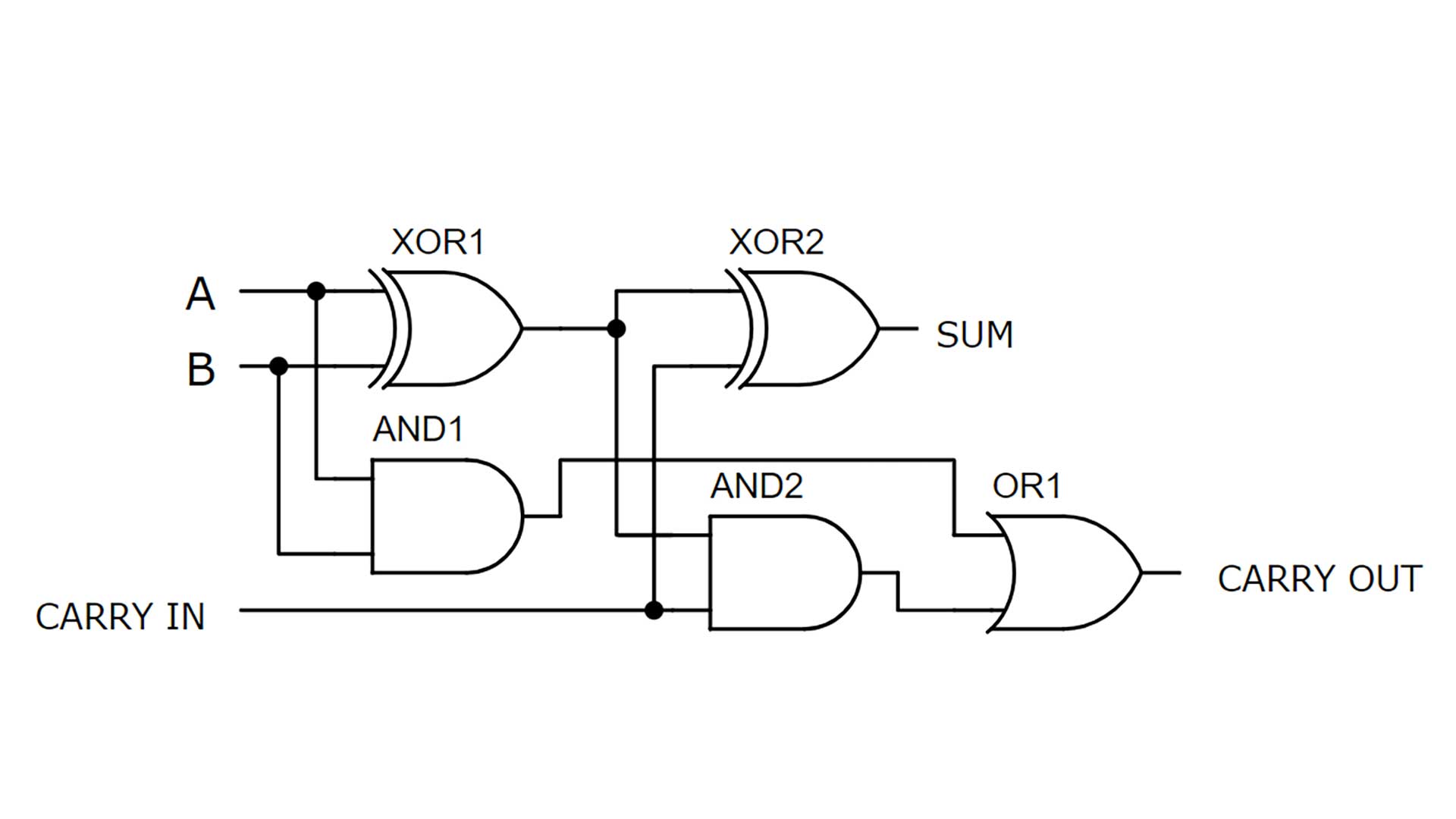
The logic gate level circuit diagram for a full adder is shown above. It is clear that 5 different logic gates are used. Inputs A and B get sent into the first XOR gate and AND gate. The carry-in gets sent to the second XOR gate and AND gate. When building larger circuits such as a 4-bit calculator the sum bit usually keeps its value while the carry-out is sent to the carry-in location of the next full adder.
Full Adder 1 Transistor Level Circuit Diagram
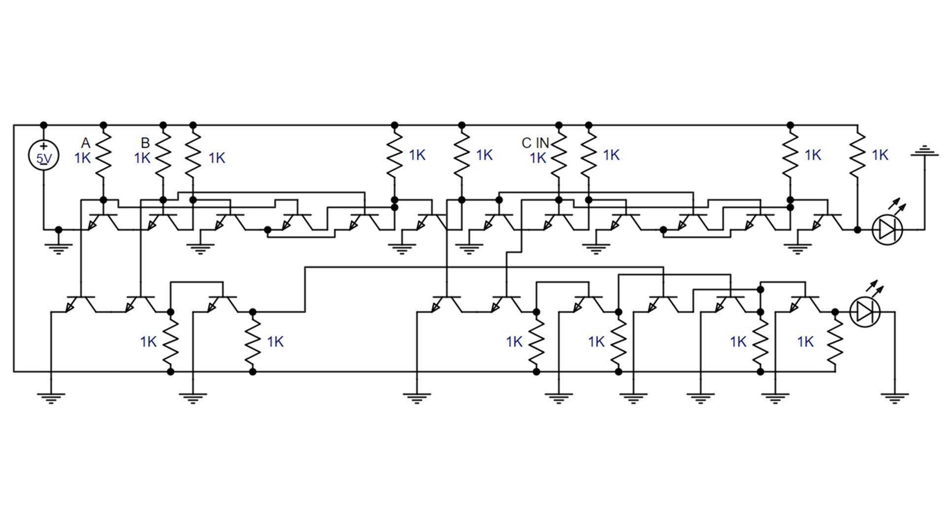
The component-level circuit diagram is often the best way to see all of the connections in the circuit. From the circuit diagram, the circuit design can be built on a breadboard or PCB. This was drawn in a circuit simulator called easyeda. Resistor values in the circuit are 1K but are 2.2K when I built them on the breadboard. This was because the simulation in easyeda ran better with lower resistor values.
Full Adder 2 Built With NAND Logic Gates
Full adder 2 is built using 9 NAND gates. Each NAND gate is built with 2 transistors so a total of 18 transistors is needed. This is the simplest and best way to build a full adder out of individual transistors. A full adder could be built using only the upper half of the breadboard, In this case, the switches did use some of the lower half of the breadboard. The resistor values used to build the actual circuit are 2.2K. In the photo inputs A and B are on and the carry-out bit is off. This is why the output value is 10 which equals two in binary.
Full Adder 2 Logic Gate Circuit Diagram
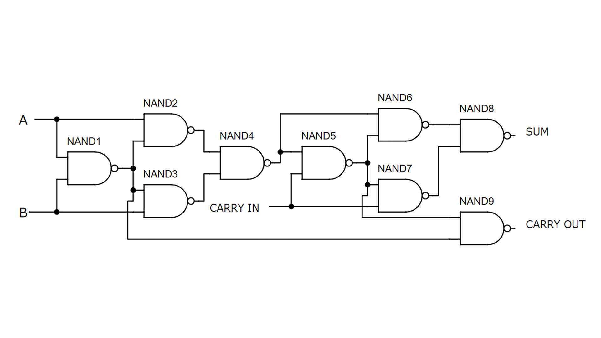
The logic gate level circuit diagram shows how the inputs and outputs should be connected for each NAND gate. When building a full adder with NAND gates you can look at the circuit I built on the breadboard or this diagram. Each NAND gate had two inputs and a single output but the output can be sent to multiple input locations.
Full Adder 2 Transistor Level Circuit Diagram
The circuit diagram shows all the connections needed to make a full adder out of 9 NAND gates. This shows all the connections need to make the circuit including the ground connections. The inputs get sent to the base of the transistors, and the output is sent from the collector side of the second transistors that make each NAND gate. Ground connections are made on the emitter of the first transistor that makes up each AND gate. Resistor values of 1K are shown but values from 330 ohms to 2.2K would work.
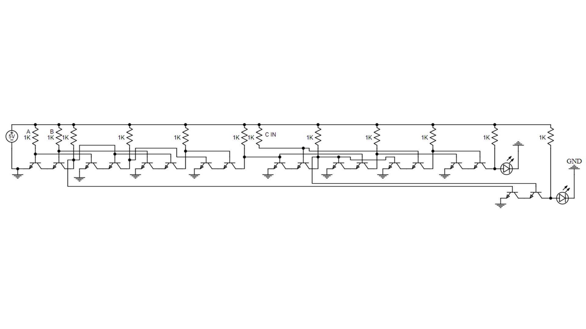
Full Adder 3 Built With NOR Logic Gates
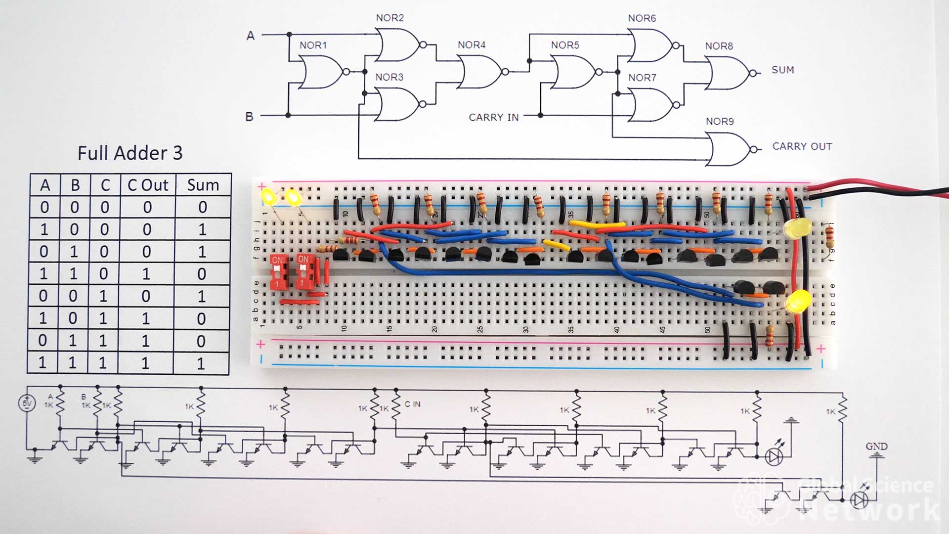
Full Adder 3 is built with 9 NOR gates. Each NOR gate requires two transistors so a total of 18 transistors is needed to make the full adder. Using NOR gates is an OK way to build a full adder on a breadboard but the wiring is a bit more complex than when using NAND gates. Each transistor in the NOR gate needs a ground. The collector of each transistor in the NOR gates is connected with an orange jumper wire. This helps the wiring to be clear and concise. The circuit in the photo has inputs A and B on and the carry-in bit off. This is why the carry-out bit is on and the sum bit is off.
Full Adder 3 Logic Gate Circuit Diagram
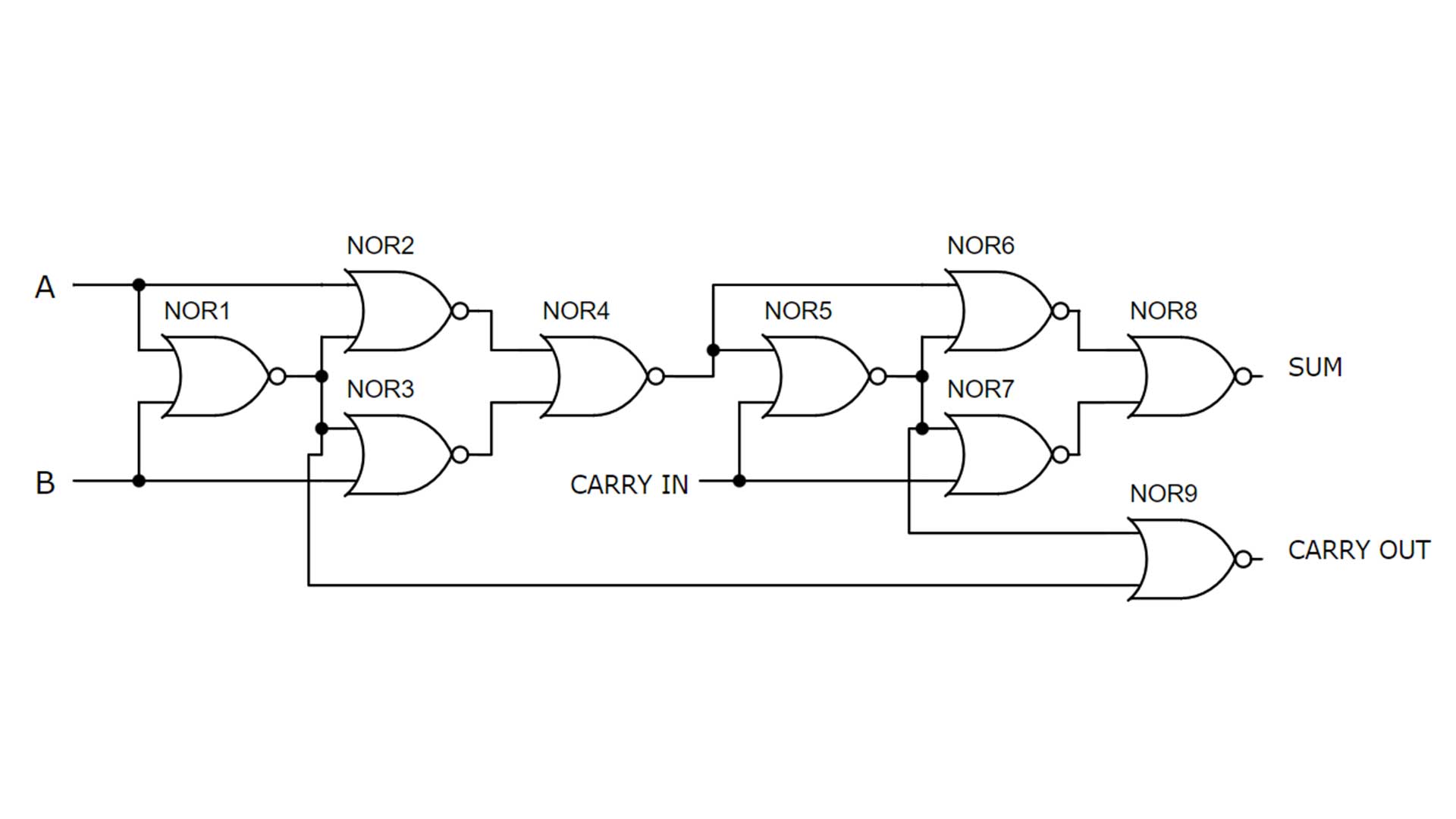
The logic gate level circuit diagram using NOR gates is shown above. It is common to look at the logic gate level drawing when outlining the circuit design. This does not give the details of how each NOR gate should be built. However, it does show how the inputs and outputs of each gate should be connected.
Full Adder 3 Transistor Level Circuit Diagram
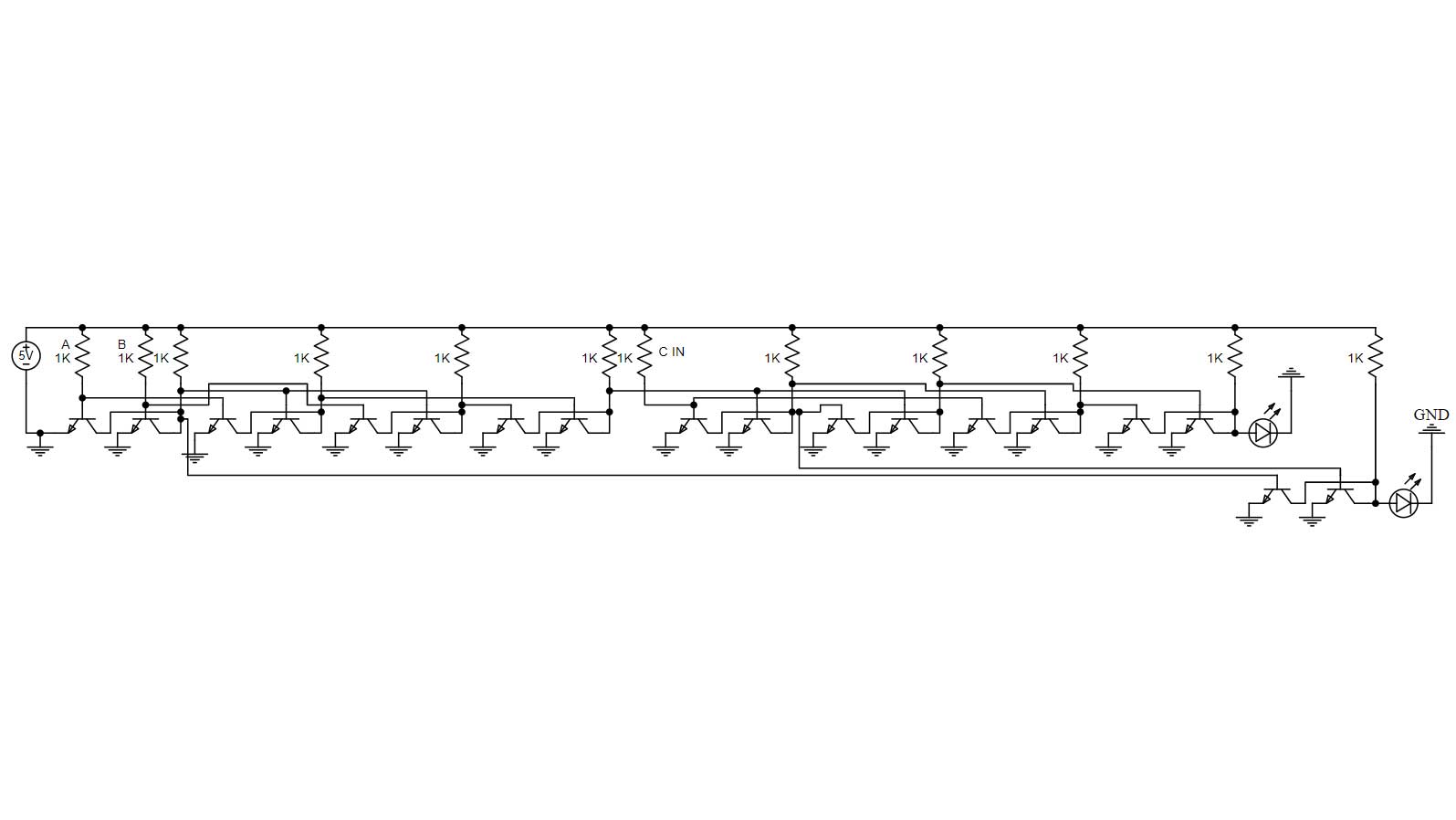
The component level circuit diagram for the full adder built with NOR gates is shown above. Overall the circuit may seem complicated but if you look at it NOR gate by NOR gate is actually pretty simple. The collector of each NOR gate is wired together. Inputs are sent to the base of the transistors and outputs are sent from the collector side of the second transistor in each NOR gate.
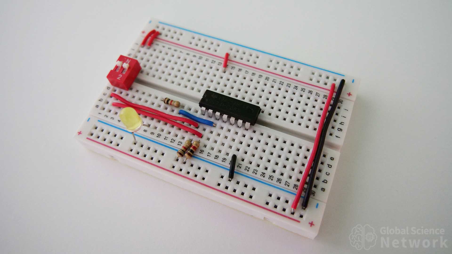
Full Adder 4 Built With Integrated Circuits
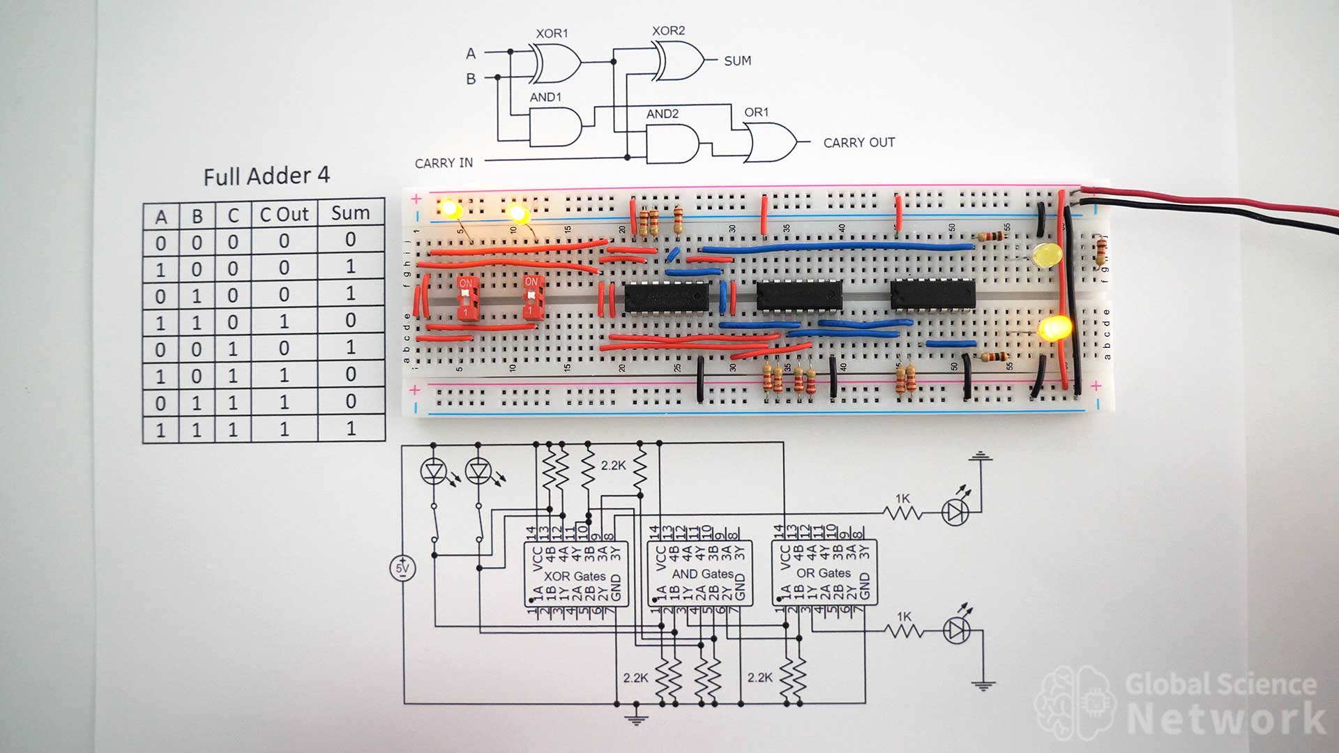
Full adder 4 is built using integrated circuits rather than individual transistors. The logic gates used are two XOR gates, two AND gates, and an OR gate. This is the same high-level design as full adder 1. The first integrated circuit had four XOR gates built on a single chip. However, only two of these XOR gates are needed to make a single full adder. The AND gate chip and OR gate chip also have four logic gates in each chip. Two of the AND gates are used and one of the OR gates is used.
Full Adder 4 Circuit Diagram with Integrated Circuits
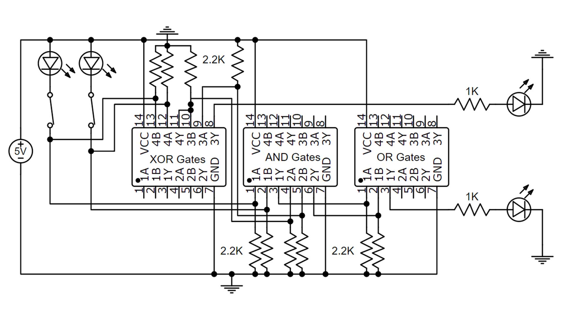
The layout of each chip is shown in the circuit diagram. Inputs are labeled A and B and the output is labeled Y. The resistor values used are 2.2 K everywhere except 1K for the outputs that connect the LEDs. Note that the first three resistors are connected to the ground, not to the positive 5-volt rail. This is because if the input is floating the integrated circuit will set it to high which means on by default. A positive 5 volts is sent to those inputs when the input is on.

Cody started the Global Science Network with the idea people should be focusing more time, energy, and resources on useful projects. He has a bachelor’s degree in aerospace engineering and a master’s degree in mechanical engineering. Cody has worked for the US federal government, a university, a large corporation, small businesses, and for himself. He has done human brain computer interface research and is currently working towards creating non-biological human consciousness.