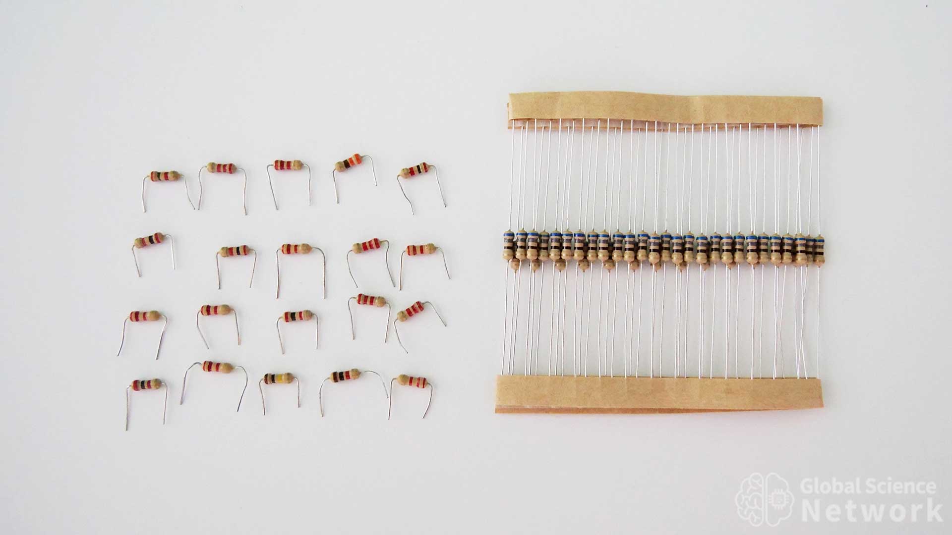
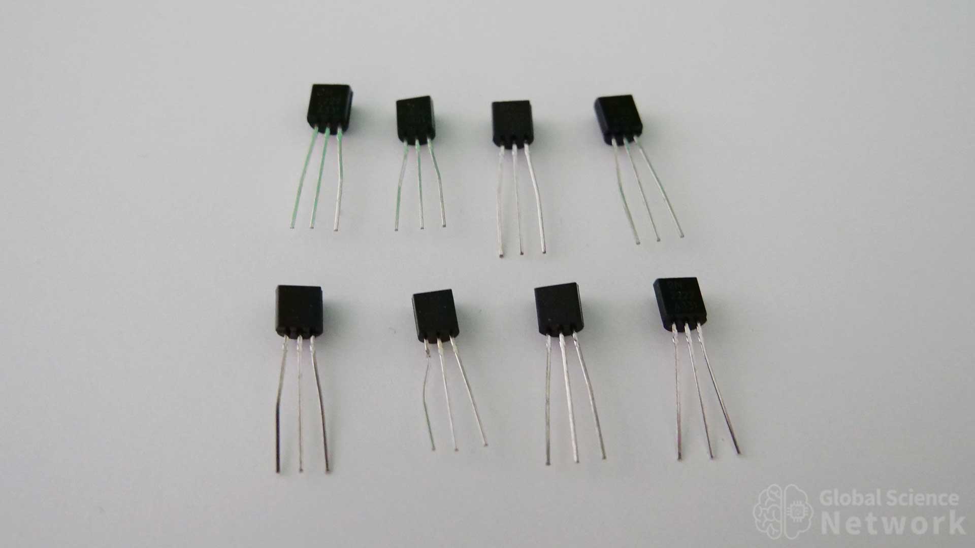
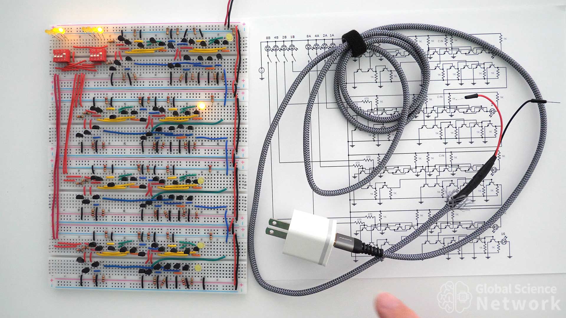
The AND gate can be made in many different ways using individual transistors. In this article, I will show 5 different ways to make an AND gate on a breadboard using individual transistors. I will also show two different ways to implement AND gates using integrated circuits. An and gate is commonly used to make half adders and full adders.
AND Gate 1
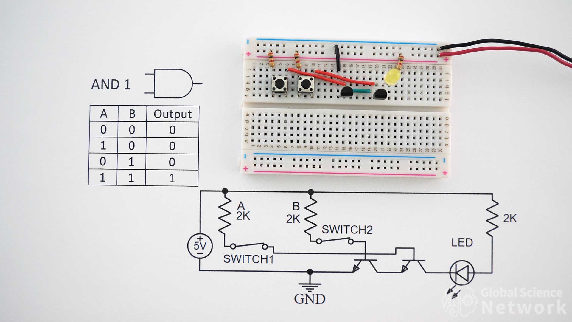
AND gate 1 is built with two push buttons switches to help demonstrate how the AND gate works. When a button is pressed current flows from the positive 5V rail into the base of the transistor turning the input on. If the button is not pressed the input is off. In the picture, neither button is being pushed so the input is off. In order for the input to be on both buttons need to be pressed down at the same time. When a button is released the output will turn off.
This video shows how to build all types of logic gates. At 16:48 the AND gate is discussed in detail. How to build AND Gates with NAND gates and NOR gates is also demonstrated.
AND Gate Truth Table
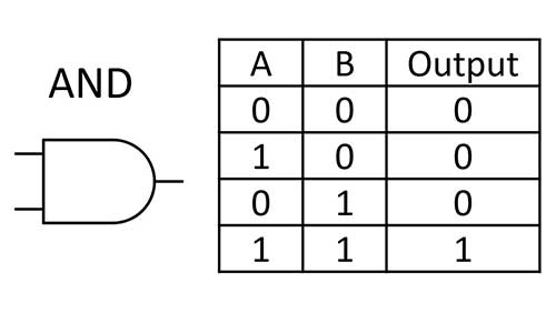
The symbol and truth table for an AND gate is shown above. It is clear when looking at the truth table that the only time the output is on is when both input A and input B are on. If no input is on or only one input is on the output will be off.
AND Gate 1 Circuit Diagram
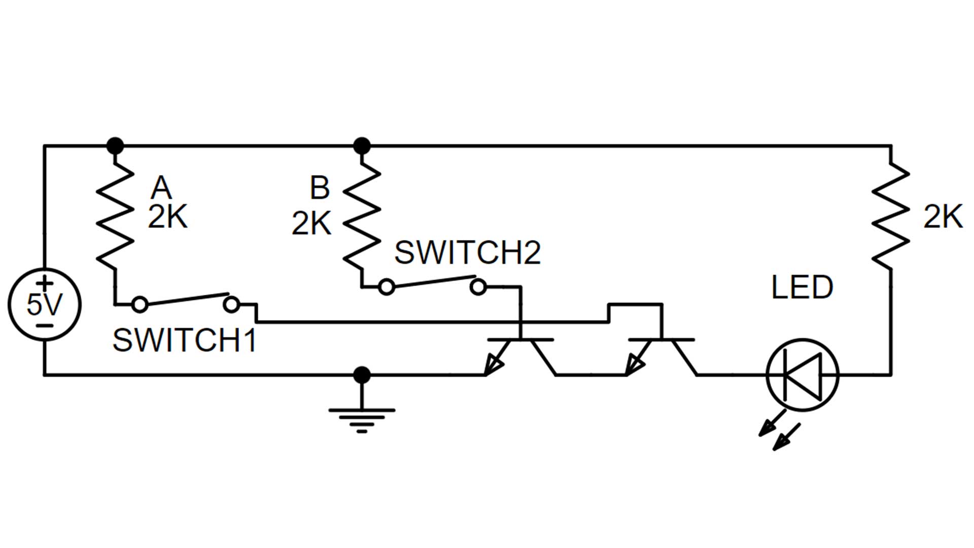
The circuit diagram above is for AND gate 1 which has the two push button switches. These switches are not required for an AND gate but help to demonstrate how the AND gate works. If the buttons are removed inputs A or B can be turned on by connecting the input resistor from the positive 5-volt rail to the base of the transistor.
AND Gate 2
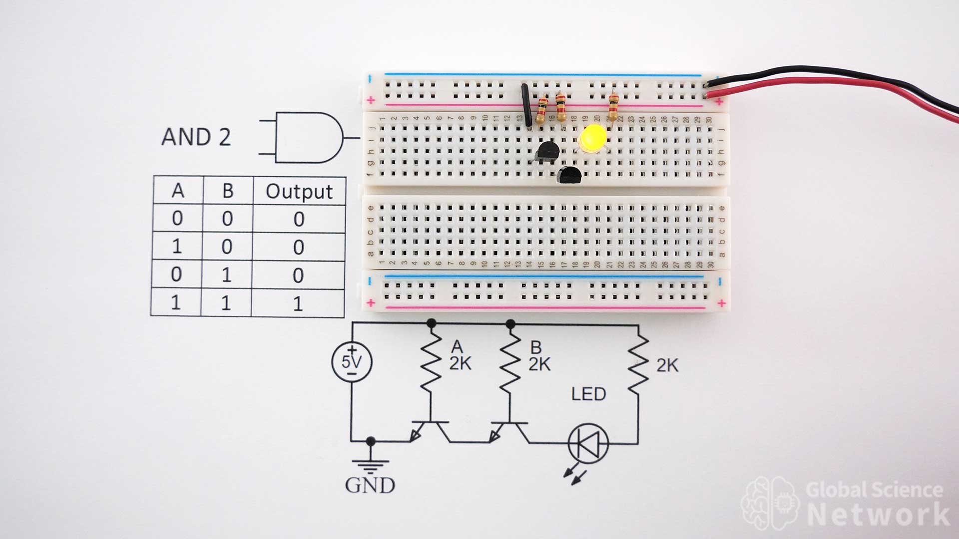
AND gate 2 is the same configuration as AND gate 1 but does not have the push button switches. Also, the collector of the first transistor is connected to the same breadboard row as the emitter of the second transistor. This makes it so the green jumper wire can be removed. Since there are no push button switches the inputs are hardwired by directly connecting the resistor from the positive 5-volt rail to the base of the transistors. This makes the configuration compact on the breadboard which is desired due to the large number of logic gates needed to implement larger circuit designs. In the photo, both inputs are ON which is why the output is on.
AND Gate 2 Circuit Diagram
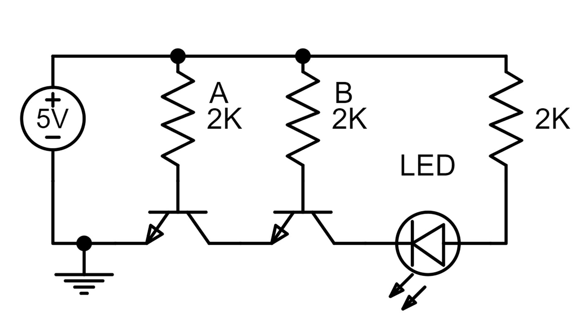
The circuit diagram for AND gate 2 is shown above. This is a simple circuit with two transistors, three resistors, and an LED. Like all the logic gate circuits it is powered with a 5-volt power supply. Note the LED direction which shows that the current is flowing into the circuit. This means that it can not be used as an output signal. However it does work as an individual logic gate or as the final logic gate in a larger circuit.
AND Gate 3
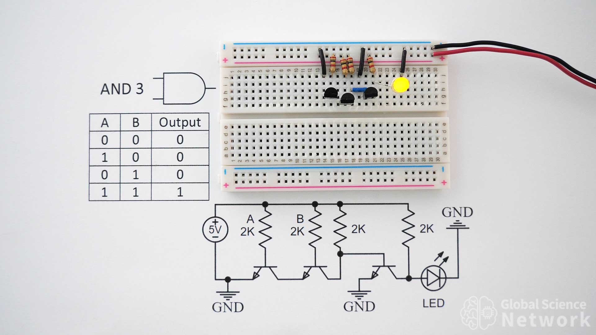
AND gate 3 is how I recommend building an AND gate using individual transistors. This is because it only requires three transistors and works in any location in a circuit. The first two transistors are set up the same as AND gate 2. However now the third transistor is configured like an inverter. The logic does not change though because the current direction also changes which is why the LED orientation is flipped 180 degrees. Now the circuit provides the desired output based on the inputs and the signal can be sent as an output. The two input resistors for input A and input B are connected in the photo which is why the output is on.
AND Gate 3 Circuit Diagram
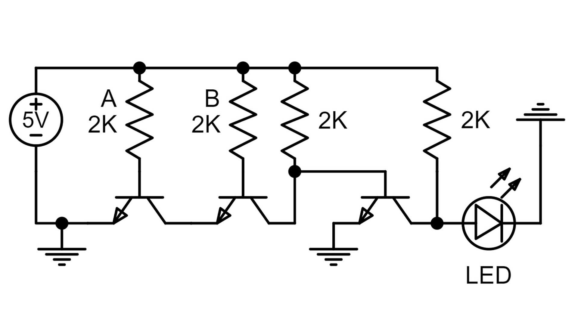
The circuit diagram for AND gate 3 is shown above. If you plan to build the circuit this allows all the connection locations to be clearly shown. All the resistor values are set to 2K. This makes it so the LED is the proper brightness.
AND Gate Built with NAND Gates
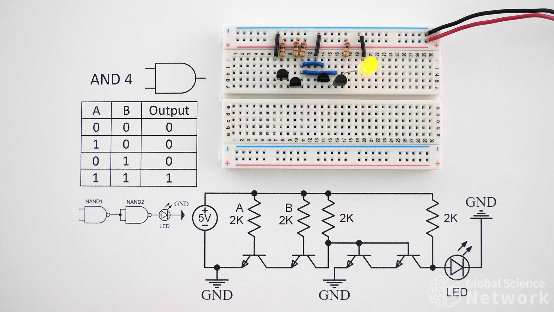
AND gate 4 is built using 2 NAND gates. Each NAND gate has 2 transistors so 4 transistors are needed to make the single gate. The blue wires connect the output of the first AND gate to the inputs of the second AND gate. Both input resistors are in place which is why the LED is lit up.
AND Gate Built with NAND Gates Circuit Diagram
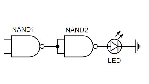
The logic gate level circuit diagram above shows the two NAD gates and their connections to make an AND gate. It is quite simple with the output of the NAND gate 1 being sent into the inputs of NAND gate 2.
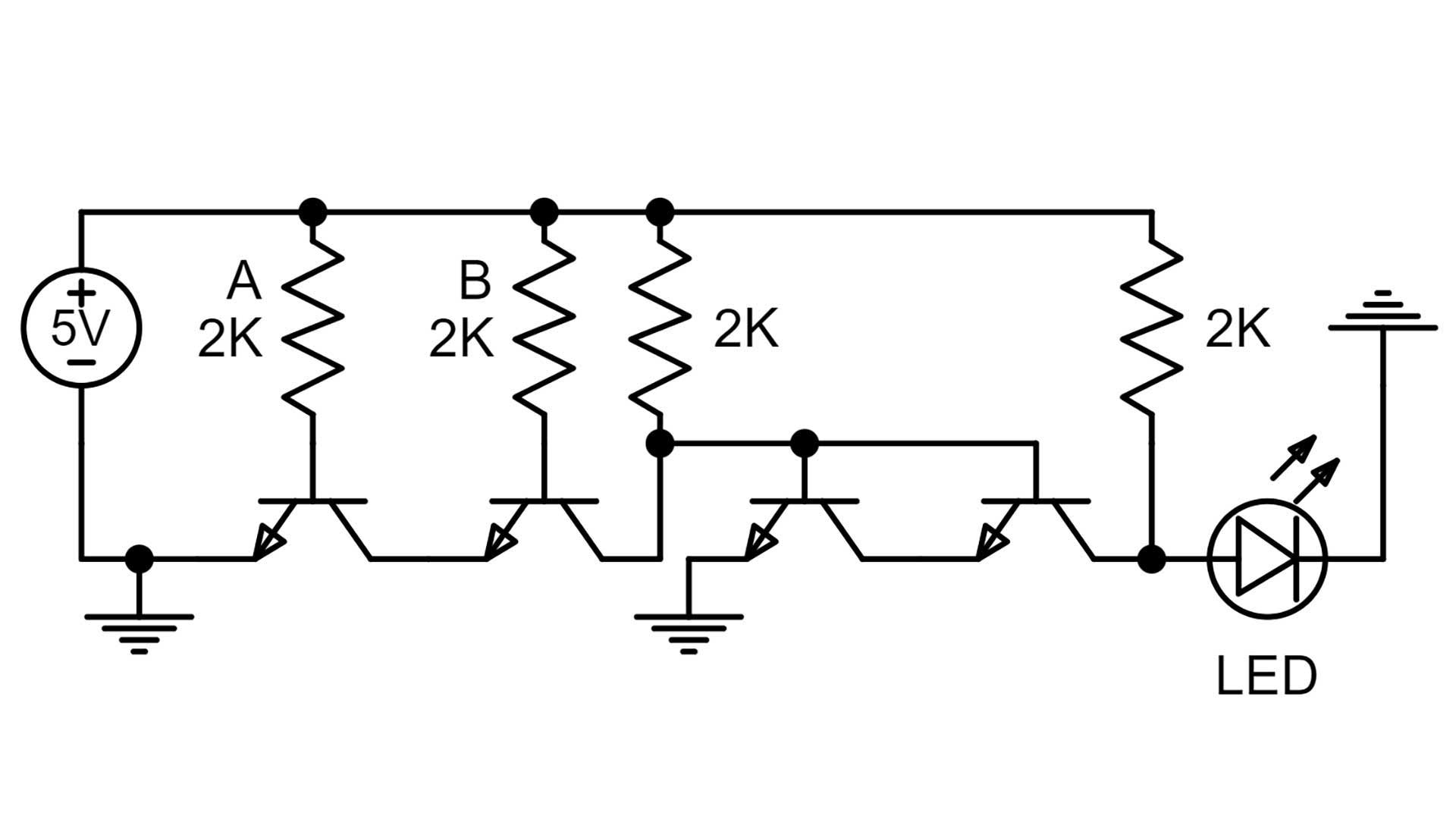
The transistor-level circuit diagram for AND gate 5 can be seen above. This shows how the resistor and connecting wires are to be connected with the emitter, base, and collector of each transistor. It also shows the ground placements and orientation of the LED.
AND Gate Built with NOR Gates
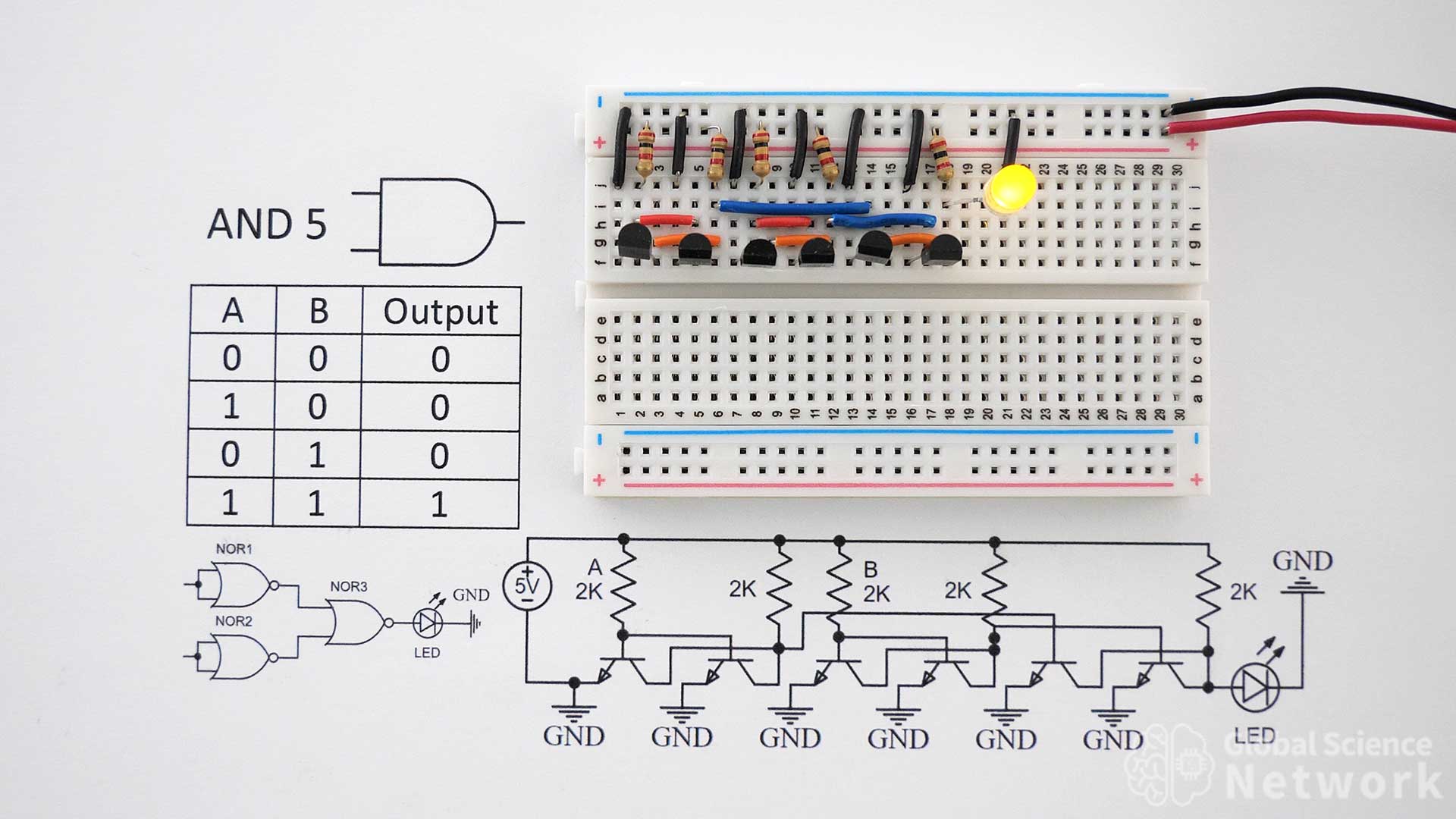
AND Gate 5 is built with three NOR gates. Each NOR gate is built with two transistors so six transistors are needed in total to make the single logic gate. The black wires connect the emitter of each transistor to the ground. Orange wires connect the collector of the first transistor to the collector of the second transistor in each NOR gate. The blue wires connect the output of the first two NOR gates to the inputs of the third NOR gate. Finally, the red wires tie a single input into both inputs for NOR gate 1 and NOR gate 2.
AND Gate Built with NOR Gates Circuit Diagram
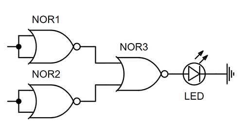
The logic gate level diagram above clearly shows how the input and output connections of the NOR gates should be made to build the AND gate. Input A and input B come in from the left and the output is sent through an LED to show that the output is on.
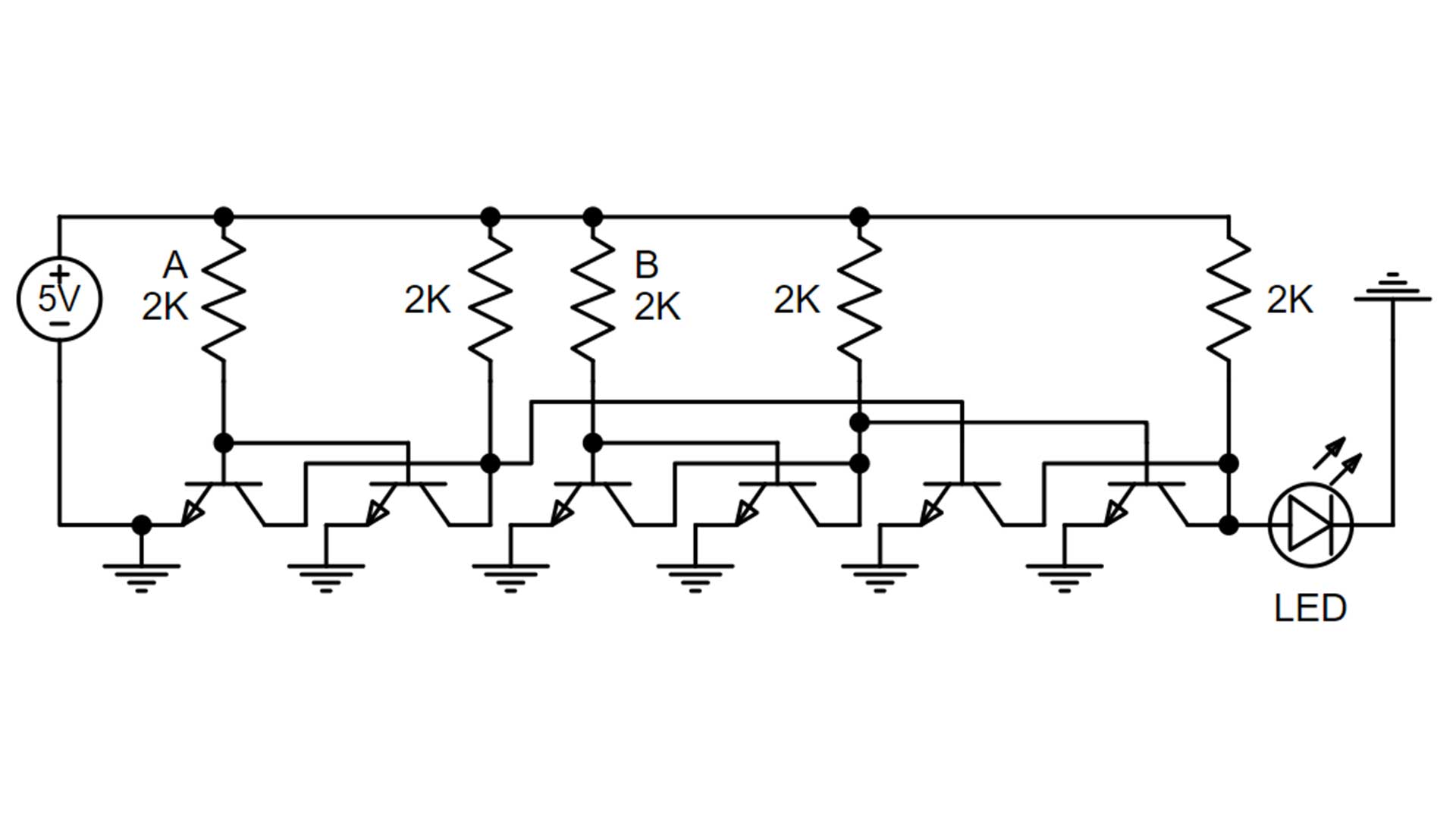
The transistor-level circuit diagram can be seen above. If it is unclear how a connection should be made when looking at the circuit on the breadboard this diagram should clarify the connection location. It also calls out the transistor values and input voltage level. This is not a commonly used way to build an AND gate but is a good option if the device is based on NOR gate logic.
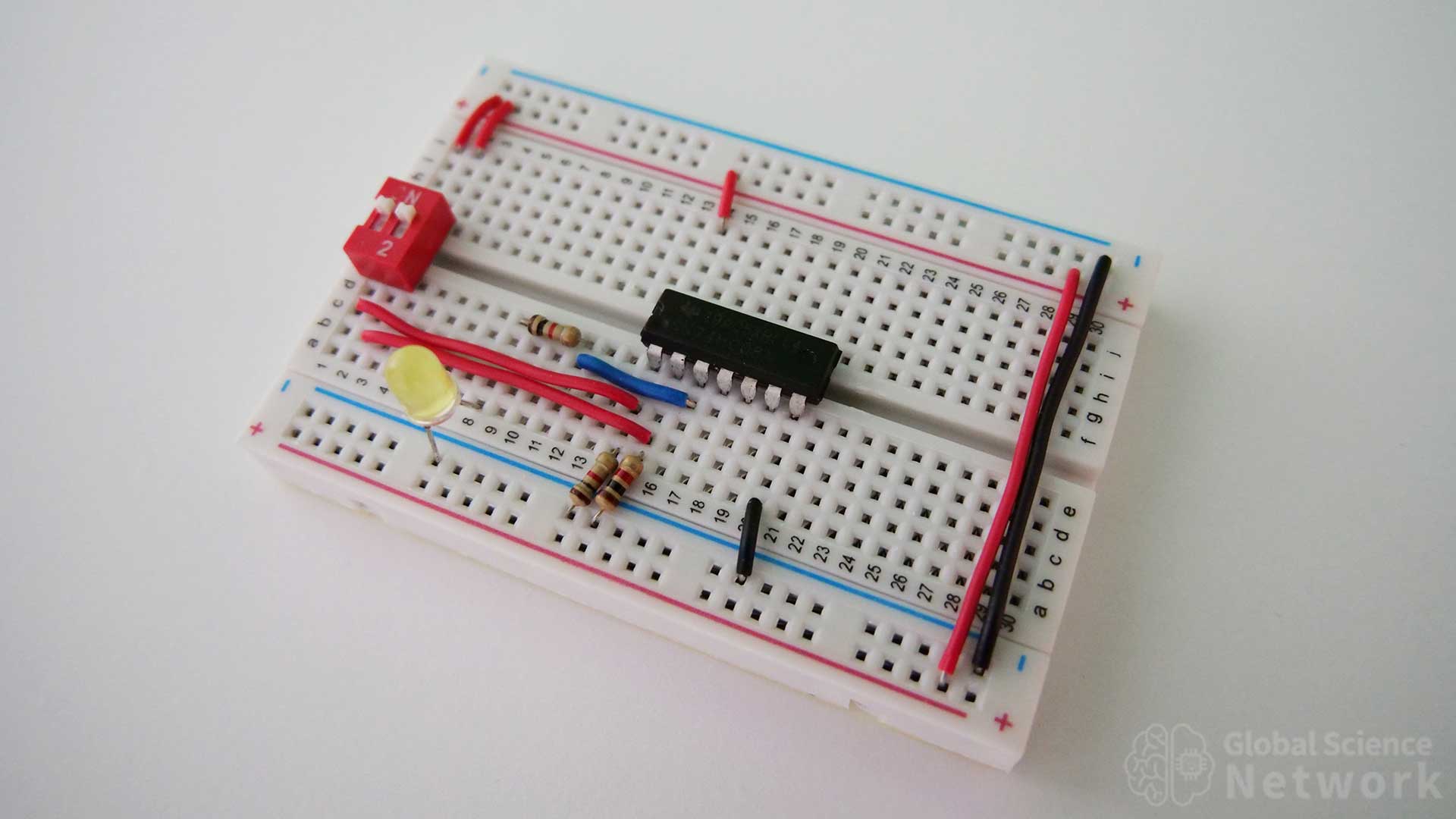
AND Gate Built with Integrated Circuits
A common way to implement AND gates is with integrated circuits. The AND gate IC has a model number of SN74LS86N. This has 4 AND logic gates and is built using bipolar junction transistors within the IC. There is a similar IC with a model number of SN74HC08N that is built with CMOS logic.
The switches for AND gate 6 shown above open paths to the ground when in the on position, rather than to the positive 5-volt rail. When the switches are closed the positive voltage is sent into the input of the IC. In the photo, both switches are closed so the output is on which is why the LED is lit up. When the switches are open the voltage drop across the resistor increases to nearly 5 volts and none of the current flows into the input of the IC. For more information watch the how-to-build logic gates video, which was previously shown in this article.
AND Gate Integrated Circuit Pinout
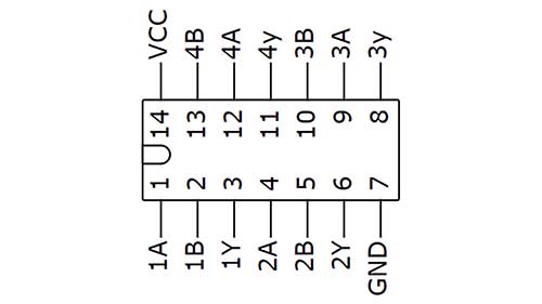
The pinout of the IC can be seen above. In the example cases, input A is pin 1, input B is pin 2, the ground is pin 7, and positive 5 volts is connected to pin 14. The output of gate 1 is 1Y which is pin 3.
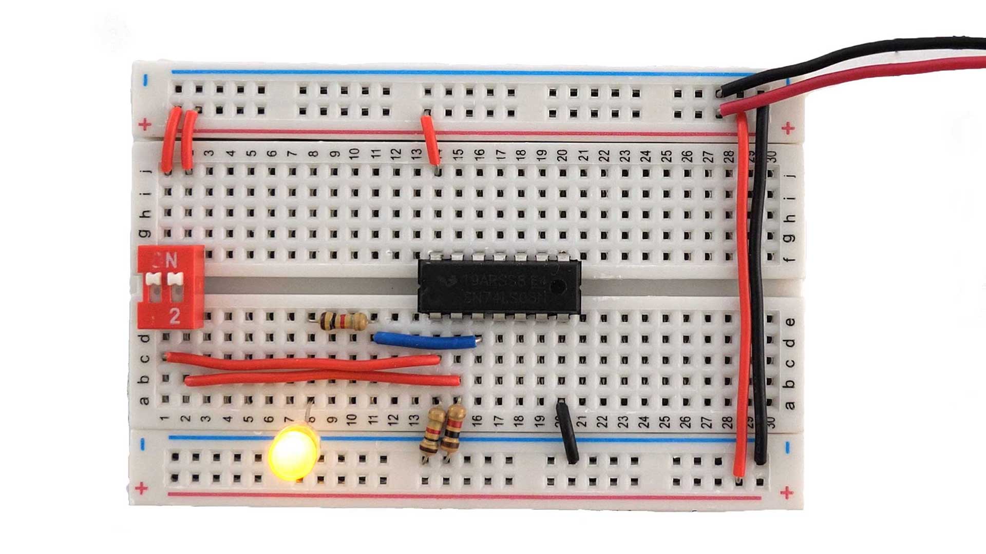
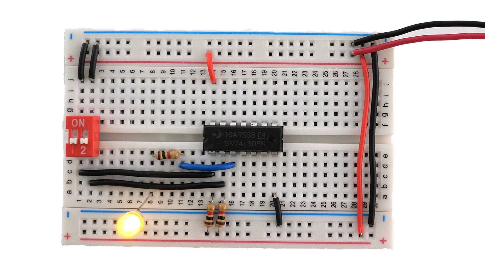
Finally, AND gate 7 is how I recommend wiring up integrated circuits. When the switches are open positive 5 volts is sent into the inputs. When the switches are closed the inputs are connected to the ground by going across the 1K resistors. If the inputs are not connected to the ground the circuit does not work properly because the inputs will set high when a positive or ground signal is not provided. This IC does have four AND gates which makes it nice and compact. However, using individual transistors is still a good way to make AND gates on a breadboard.

Cody started the Global Science Network with the idea people should be focusing more time, energy, and resources on useful projects. He has a bachelor’s degree in aerospace engineering and a master’s degree in mechanical engineering. Cody has worked for the US federal government, a university, a large corporation, small businesses, and for himself. He has done human brain computer interface research and is currently working towards creating non-biological human consciousness.