Breadboards are used to build and test electrical circuits. These are used by hobbyists and professional electrical engineers. Using a breadboard allows for electrical connections to be made without using solder which is why they are also called solderless breadboards. Not having to make a permanent connection with solder makes it so the placement of wires and discrete components such as resistors, LEDs, and transistors can be easily changed.
A breadboard is typically used in the prototyping stage of a circuit design. This makes it so that mistakes can be made without having to build an entirely new printed circuit board (PCB). Different designs can be tested quickly with almost instant results. Sometimes it is easier to design circuits in a circuit simulator. However, at some point in the circuit design, it should be tested with actual components to verify it works as expected. Once a final design is made on a breadboard it can then be made on a PCB which makes the circuit smaller, and easier to mass produce.
Buy from Amazon
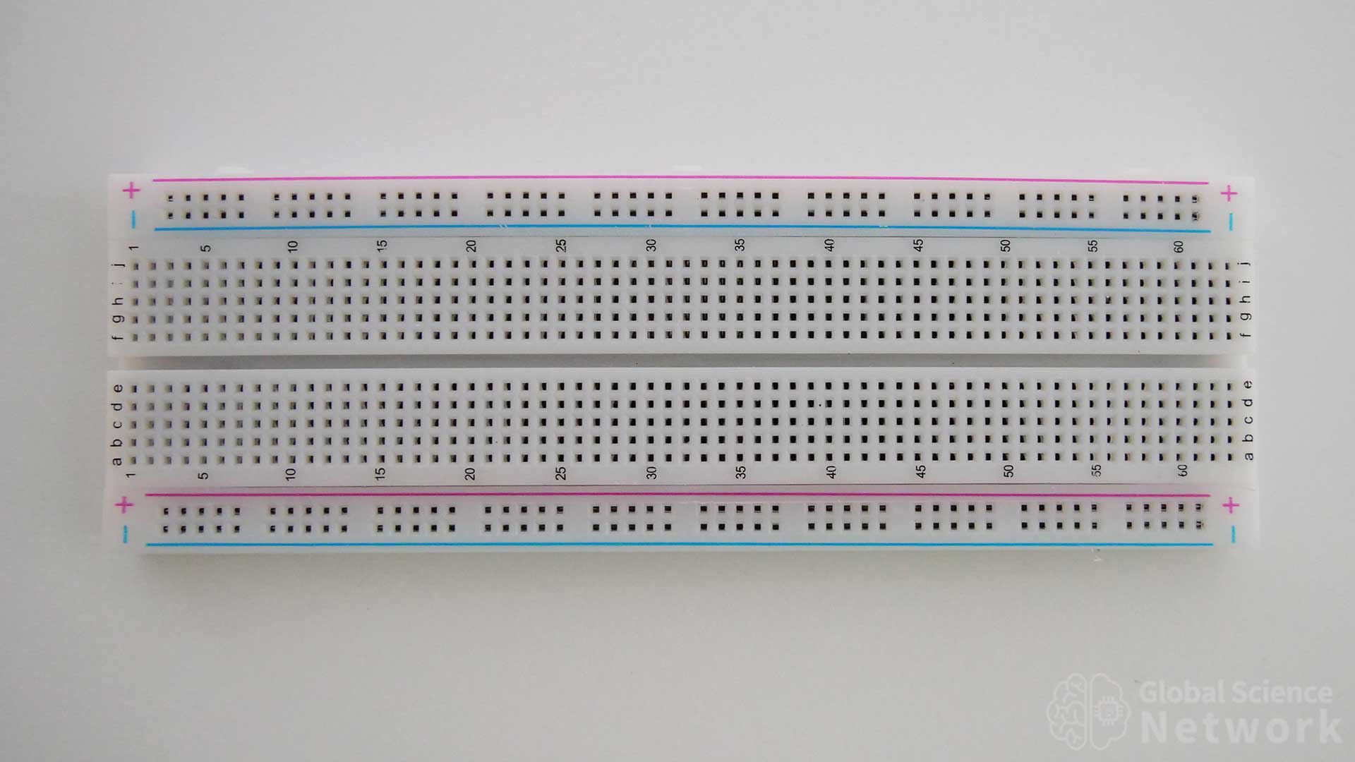
There are several different size breadboards but each one is built in a similar way. Power is supplied to the power rails which run along the outside of the breadboard. The power rails are horizontal rows. On the inside, there is a grid of holes where the rows are labeled a-j and the columns are numbered 1-60. The holes in the power rail rows are electrically connected but the rows on the inside are not electrically connected. Vertical columns are electrically connected between rows a-e and rows f-j.
The power rails are labeled + and – for where the positive and negative terminals of the power supply should be connected. Multiple breadboards can be connected together by sliding the tabs of one breadboard into the grooves of another. A breadboard can also be secured to a flat surface as the bottom has a sticky layer that can be exposed by removing the paper backing.
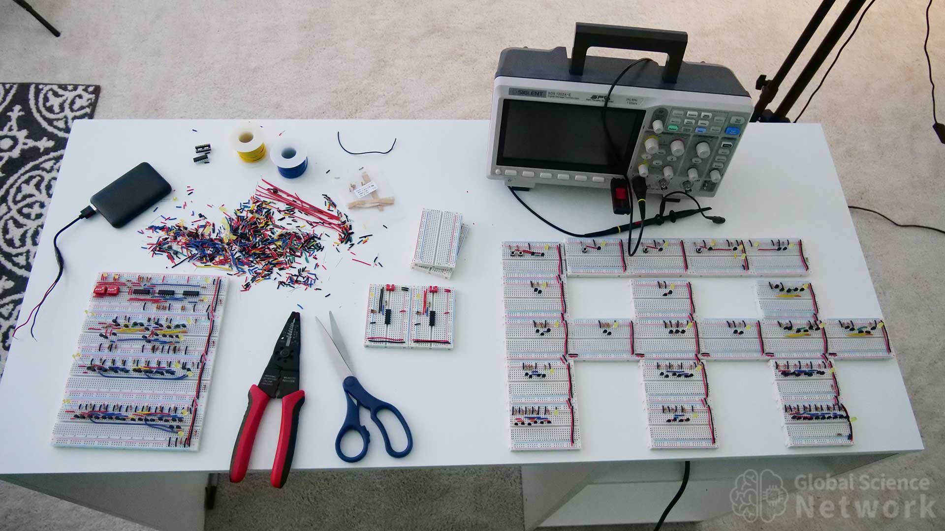
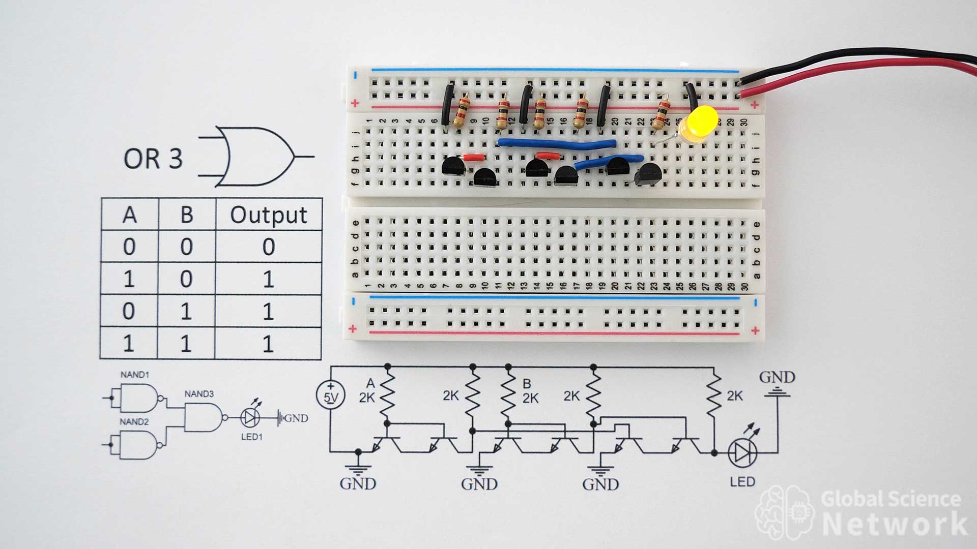
In the photo above I am working on multiple breadboard projects involving digital logic gates. An oscilloscope is used to measure voltages within the circuits. On the desk, there is a large number of cut wire scraps as each wire is custom cut to length. Both full-size and half-size breadboards are being used.
Breadboard Components
Wire
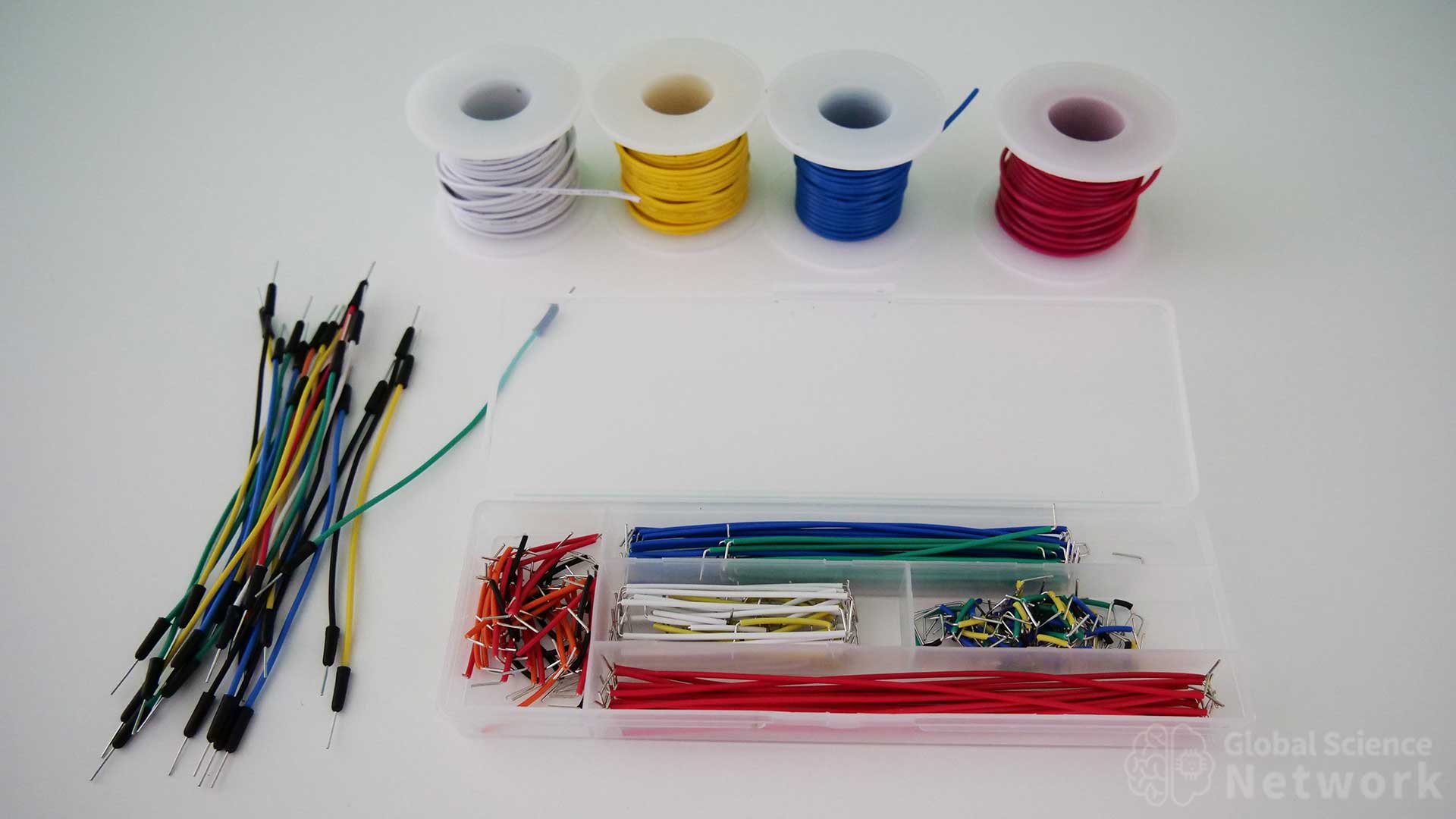
There are three different types of wires used for breadboarding. These are jumper wires, spools for wire, and pre-cut wire. Each will be discussed in detail below.
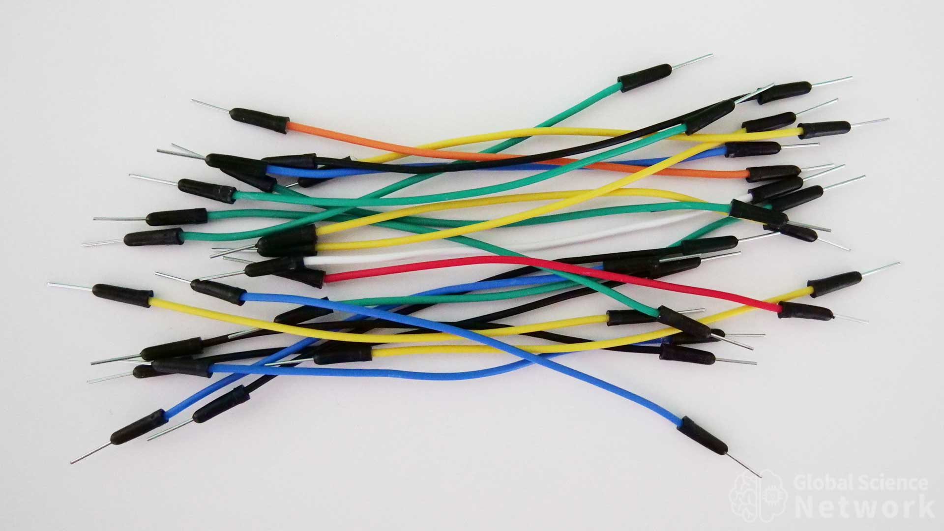
Flexible jumper wires are the quickest and easiest way to make a wire connection on a breadboard. These are made with multistrand wire with a PVC coating. Multistrand cable is flexible but does not fit well into breadboard holes. For this reason, there are metal pins on the end that fit properly into the holes of the breadboard. The disadvantage of using jumper wires is the extra length of wire makes it less clear where each wire is going to and from. This is especially true when lots of wired connections are made. Jumper cables are great for quick testing but are not to build circuits to take pictures of and show circuit designs to others.
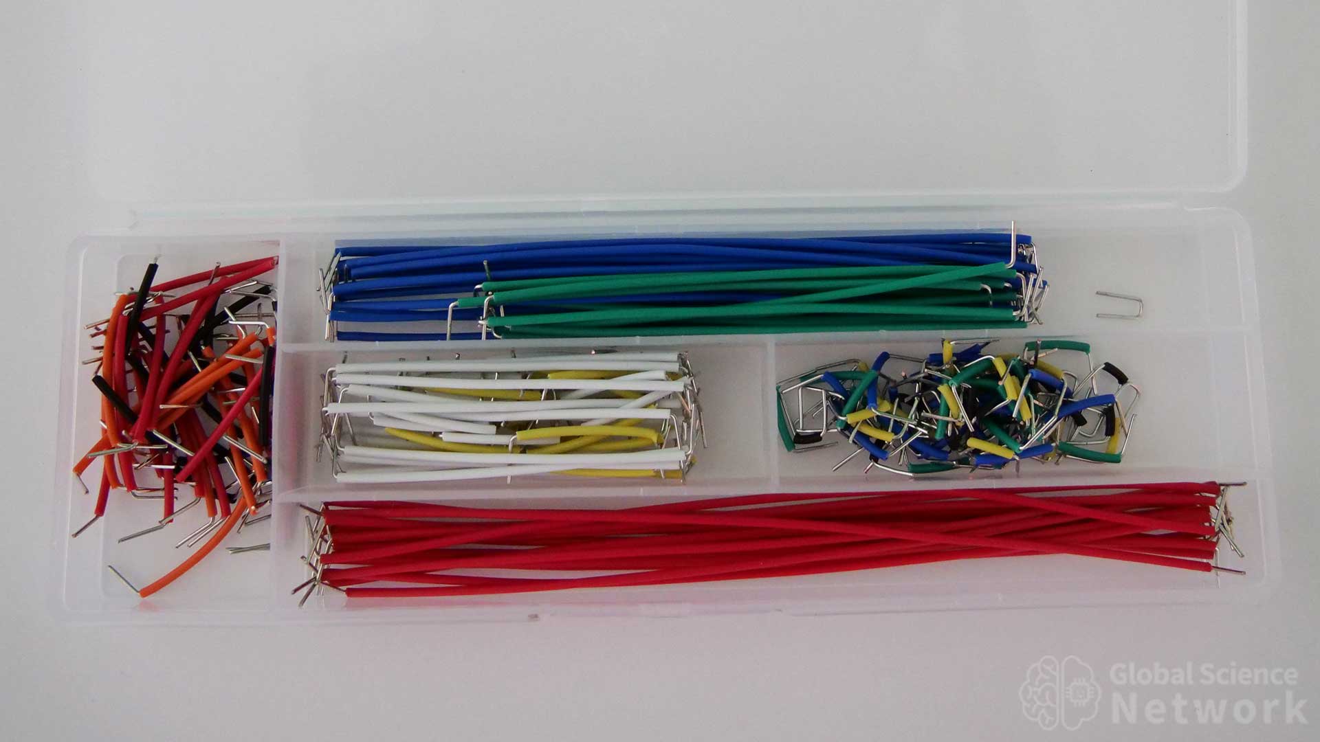
Precut wires can be nice because the wires are cut and bent to specific lengths. This does help speed up the process when breadboarding. The problem is that the wires are color coated based on length. Often times when building circuits it is nice to color code the wires based on the connection type. For example black going to the ground, red going to the positive rail, blue wires sending data, etc. I do use precut wire when the wire I need is shorter than the precut wire. This way I can cut it down and still use the color I want. It saves some time as one end is stripped and bent already.
Buy from Amazon
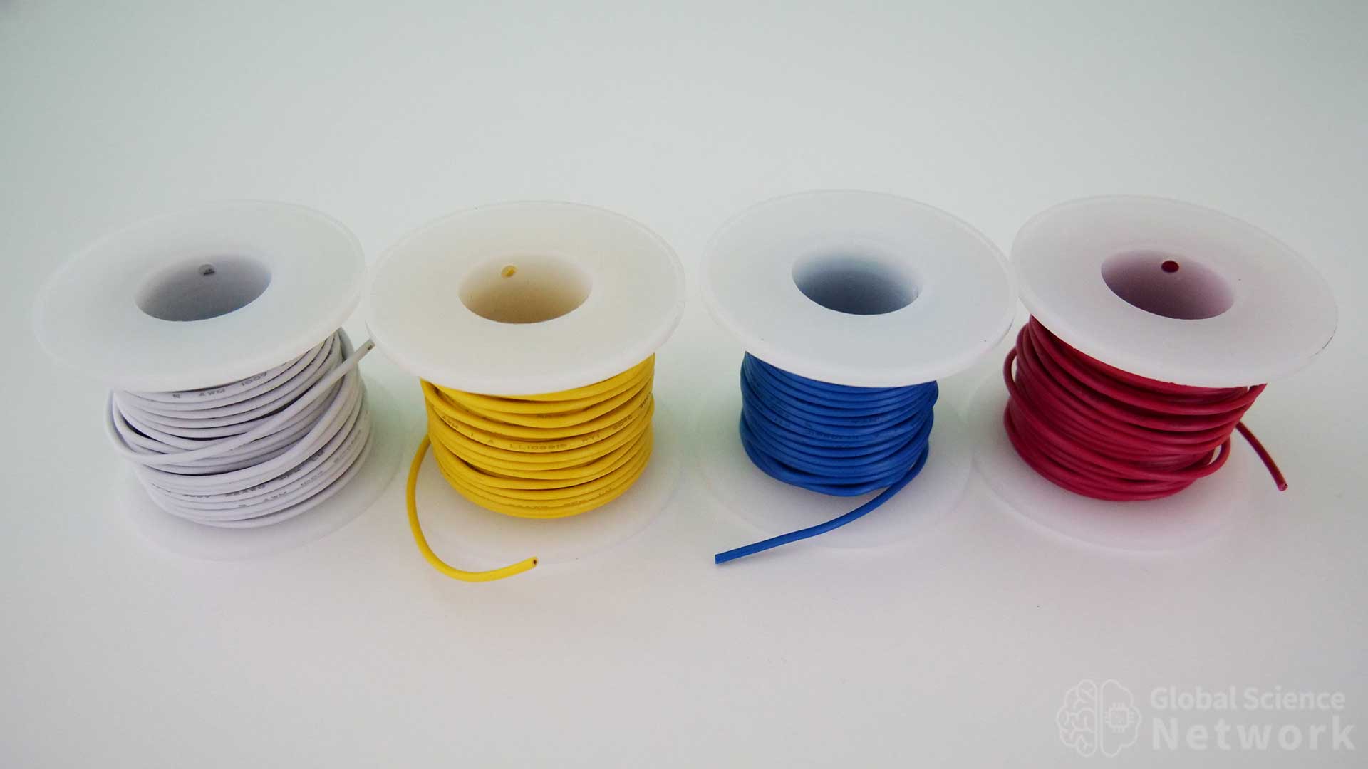
The best wire to use for breadboards comes on spools. It is a 22 gauge solid core wire. Each spool has over 25 feet of wire. Common wire colors are red, black, yellow, blue, white, and green. The disadvantage of the wire spools is that each wire needs to be cut to length and stripped on both sides to expose the wire. When this is done properly it makes for a very nice-looking circuit where it is easy to see where the wires are going to and from. So it is often worth the extra time. Each wire should be cut so that it lays flat and the stripped ends fit securely in the holes.
Resistors
Buy from Amazon
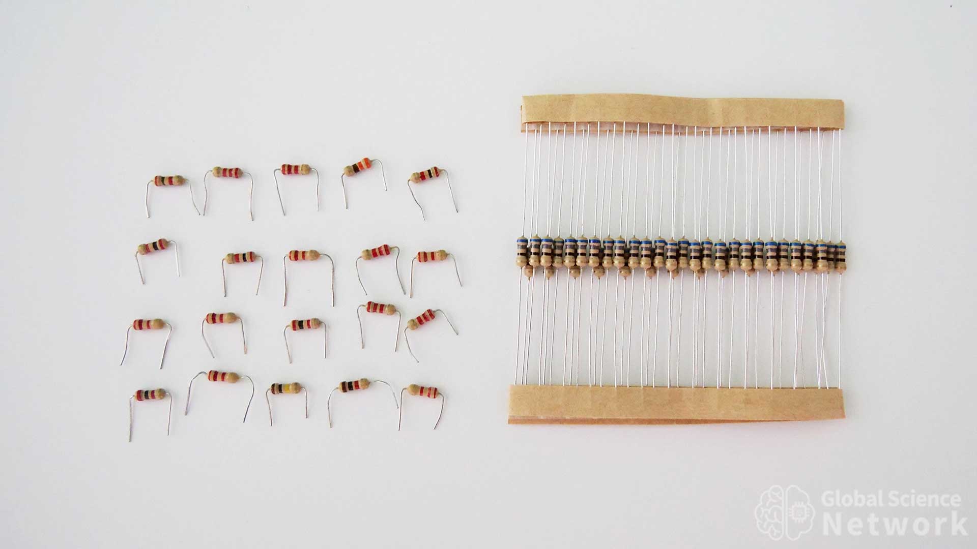
Resistors are one of the most common components used when breadboarding. Each resistor is marked with color-coated bands to display its value. Common resistor values used for breadboards range from 1 ohm to 1 mega ohm which is 1 million ohms. Often times the exact value of the resistor is not needed so one with a slightly higher value should be used. For example, if your calculations show you need a 945-ohm resistor, using a 1K resistor will work in most cases.
Resistors come with long wires on each end that need to be cut and bent to fit properly in the breadboard. The full length can be used but in most cases, this will make the resistor sit high above the breadboard. Having resistors lie flat makes the breadboard look more organized and is easier to see where connections are being made.
LEDs
Buy from Amazon
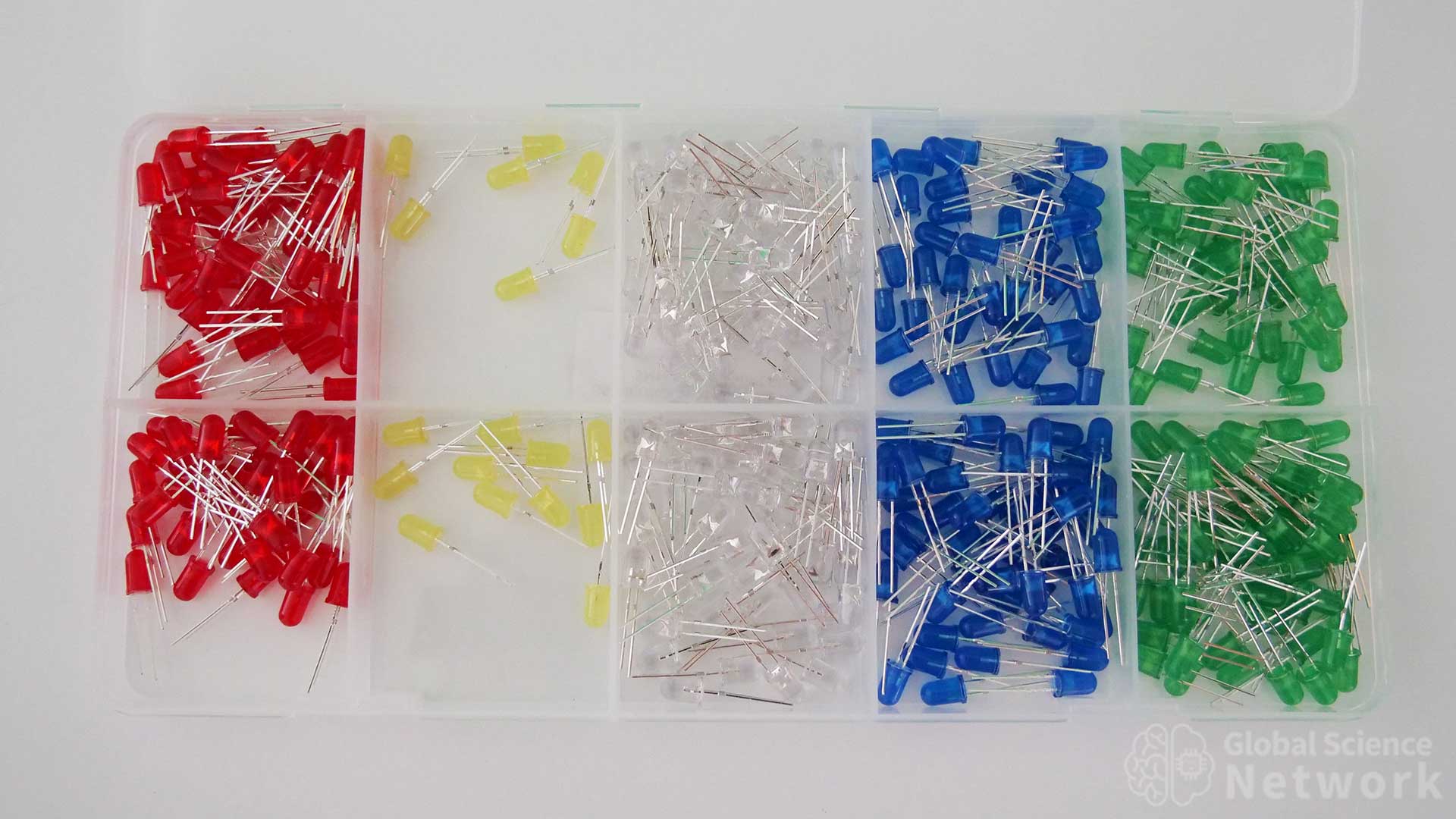
LEDs are often used in breadboards to show that the power is on. Using an oscilloscope or multimeter can provide the exact power value. However, often times it is advantageous to just see that power is on. Also, the brightness of the LED gives insight into how much current is being applied across the LED. When using LEDs it is important to have a current-limiting resistor or the LED can be damaged.
Most LEDs have a voltage drop ranging from 1.8 volts to 3.2 volts. This is different from standard diodes which have a voltage drop of around .6 volts. The common input voltage for breadboards ranges from 3 volts to 9 volts. If the resistor is larger than 350 ohms it should limit the current to less than 20 milliamps. The max current rating for LEDs is typically 20-25 milliamps. Common colors for LEDs are red, yellow, white, blue, and green.
Transistors
Buy from Amazon
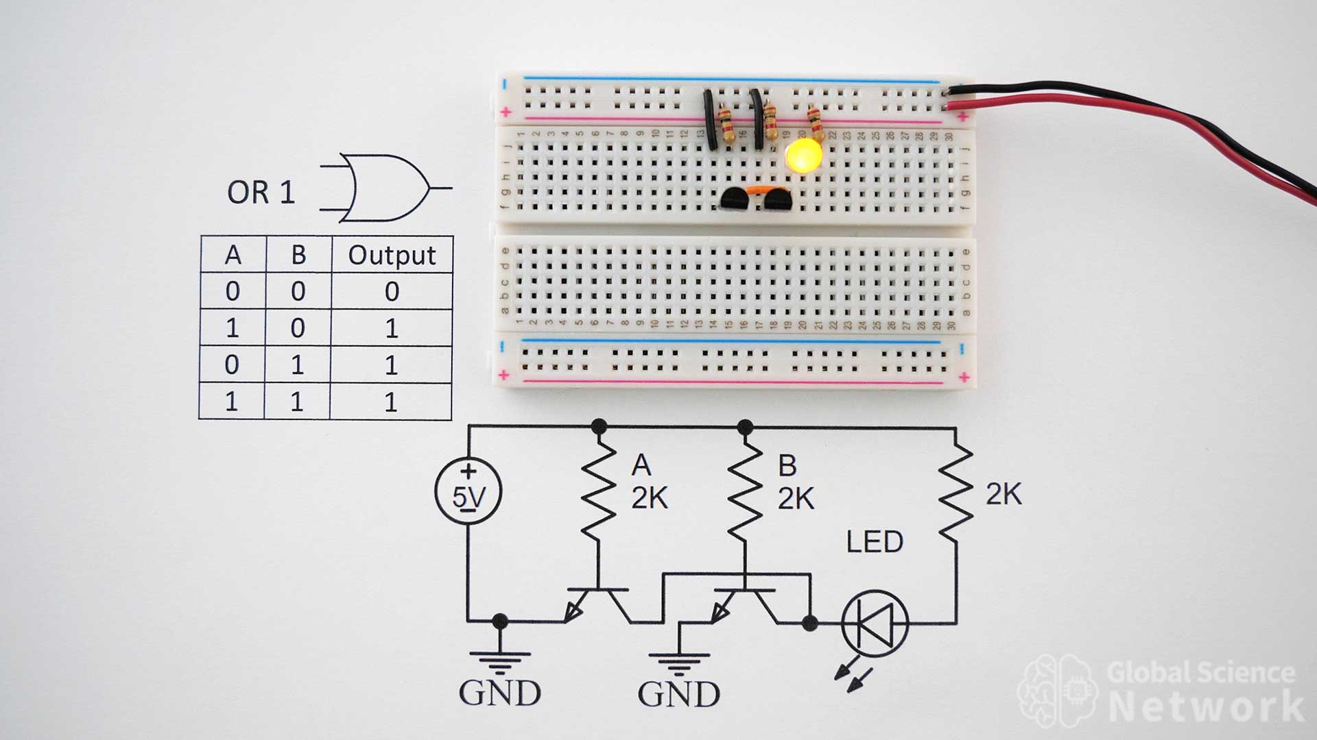
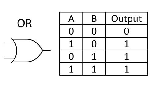
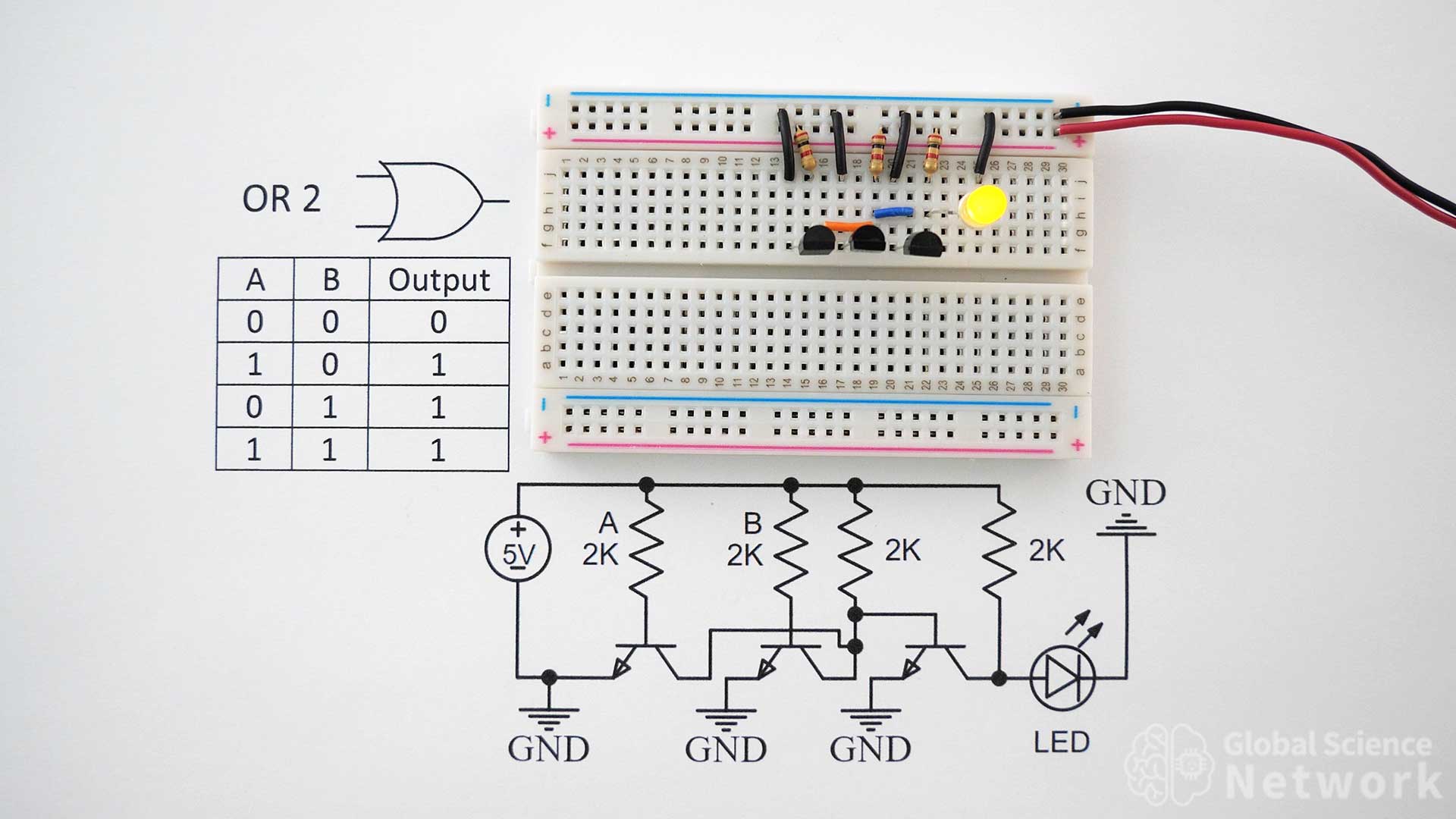
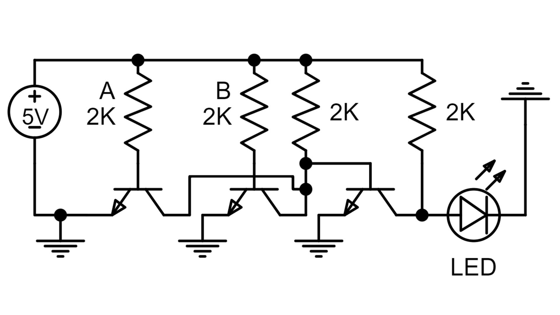
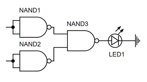
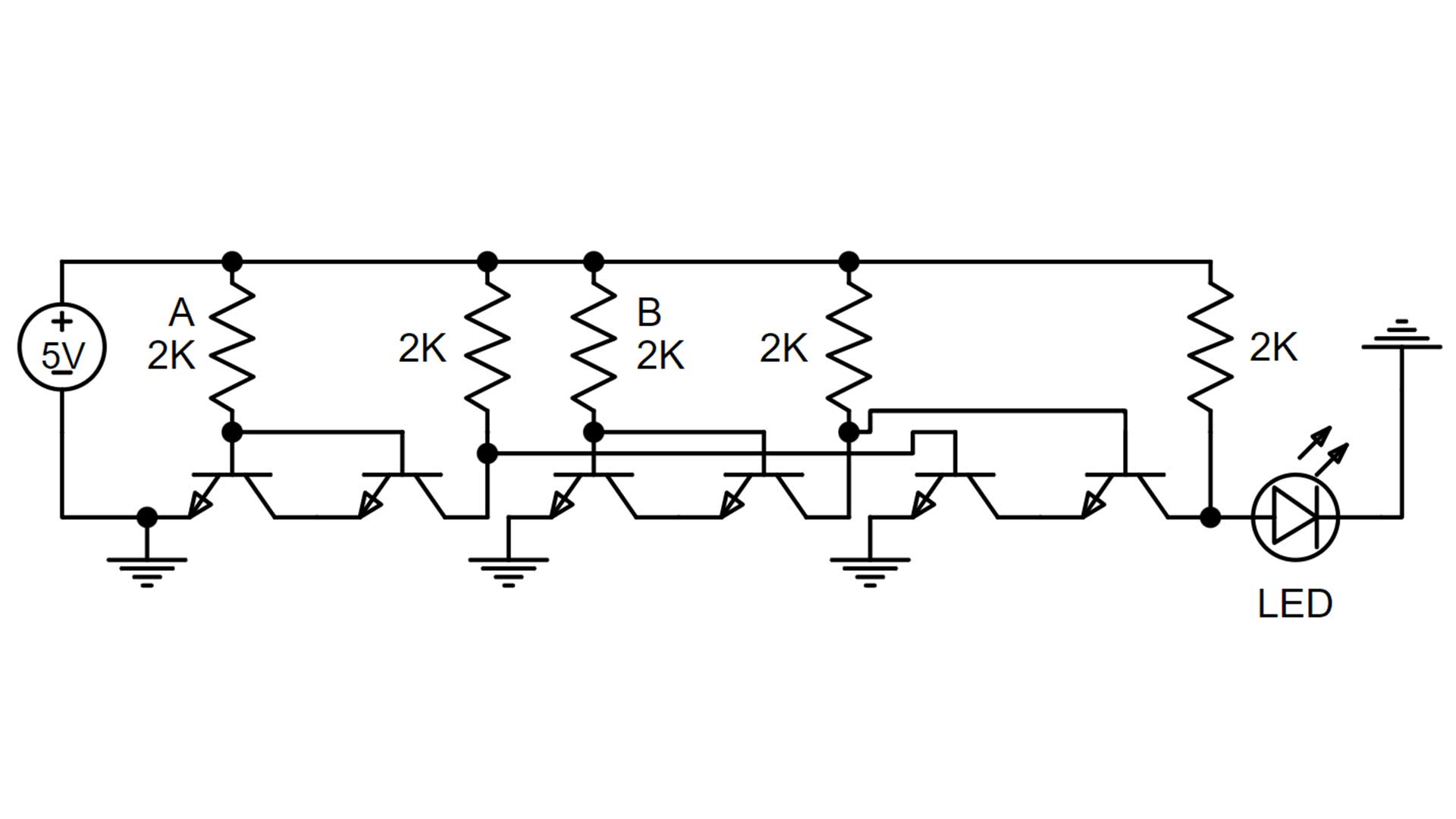
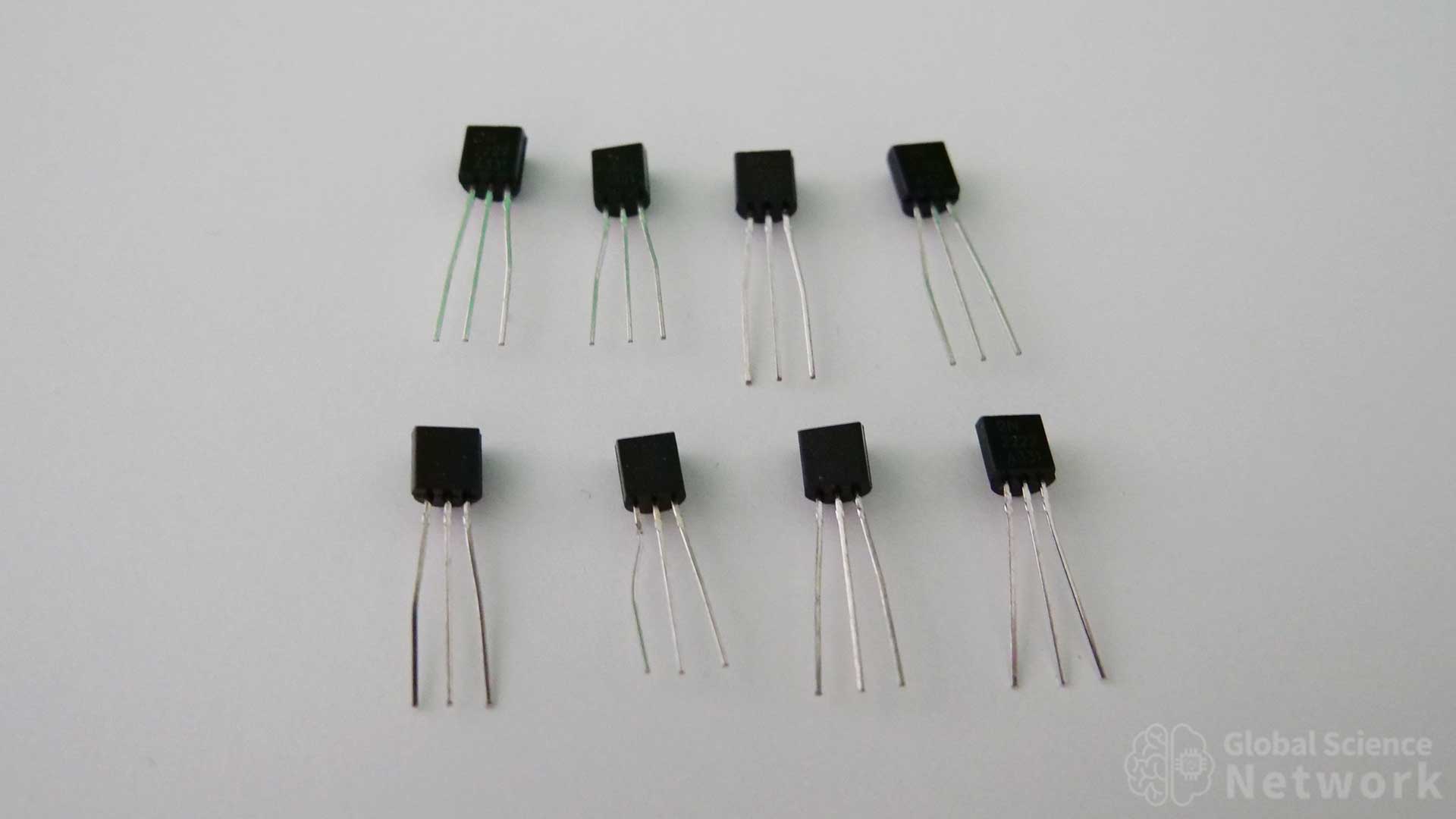
BJT transistors have three pins that are designed to work with breadboards. The three pins are the emitter, base, and collector. Which pin is which will vary depending on if it is an NPN or PNP transistor. The most common transistor used with breadboards is the 2N2222 NPN transistor. This is an amplifying transistor and also works as a switching transistor. I have used these to build digital logic gates. Like LEDs, transistors should also have a current-limiting resistor to prevent damage.
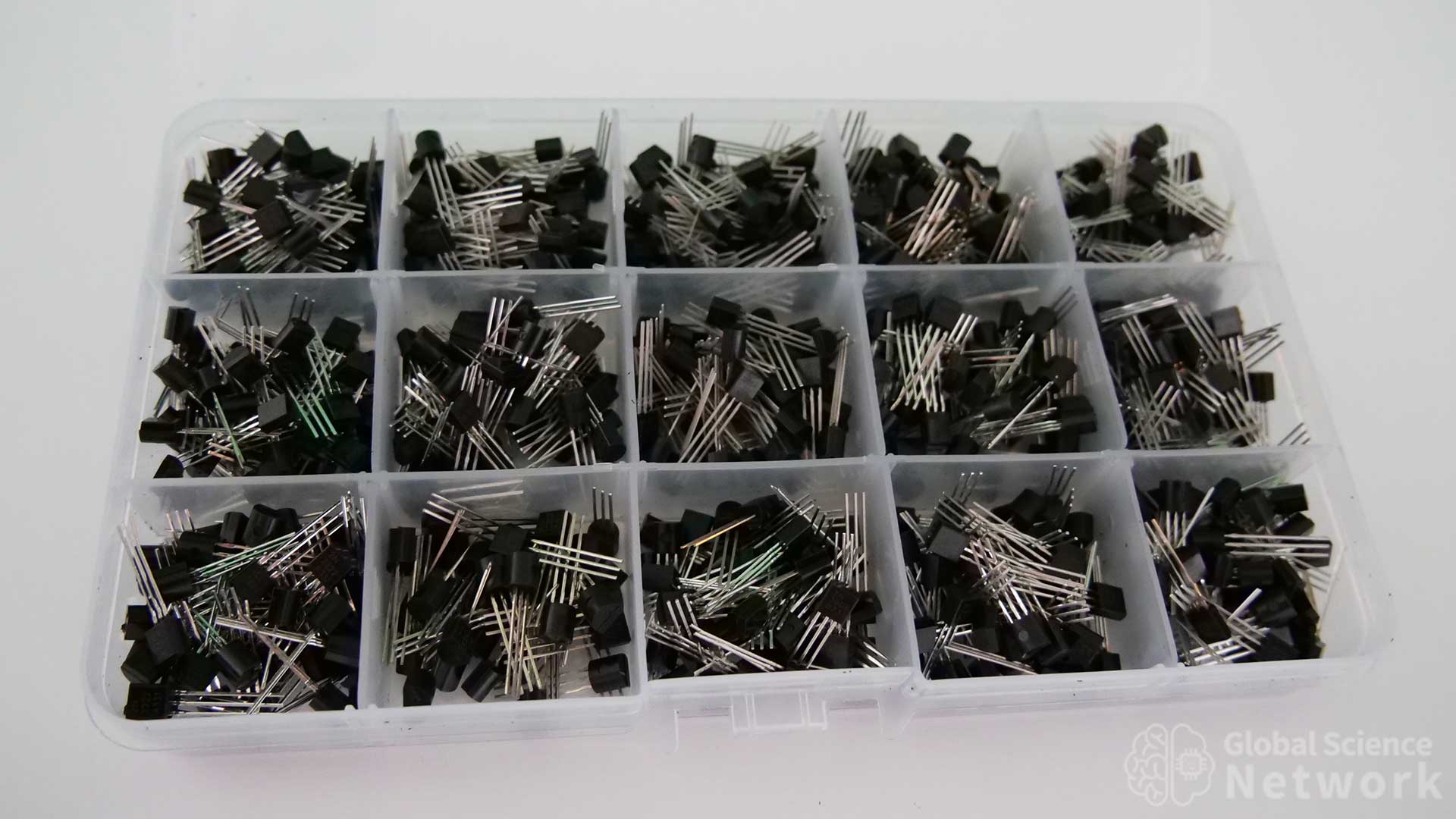
Transistors often come in large sets where the are many types of NPN and PNP transistors. The most common NPN transistors are the 2N2222 and the 2N3904. For PNP transistors the most common are the 2N2907 which is equivalent to the 2N222 and the 2N3906 which is equivalent to the 2N3904. Each transistor does have different specifications so using the proper model number is important.
Capacitors
Buy from Amazon
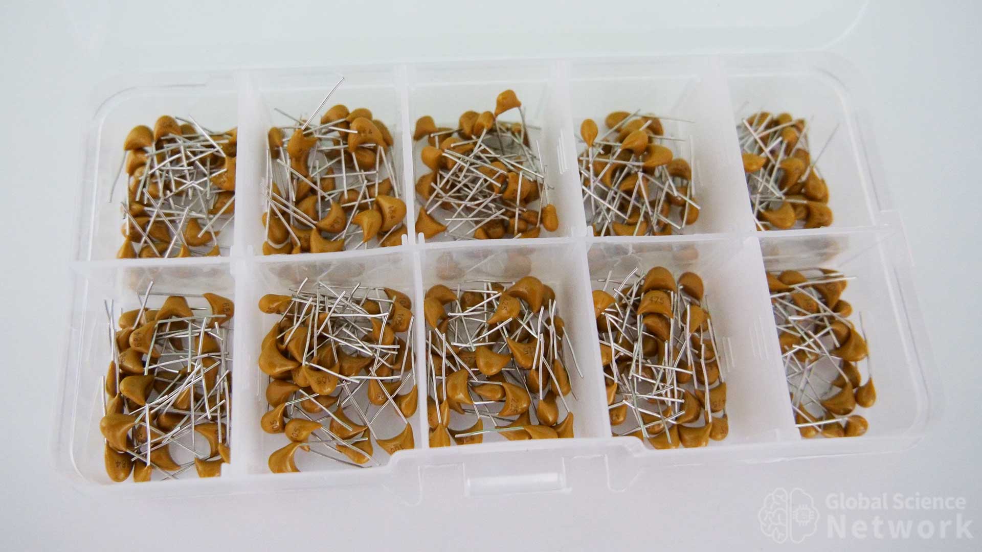
The three types of capacitors used with breadboards are ceramic capacitors, aluminum electrolytic capacitors, and metalized polypropylene capacitors which are also called film capacitors. In the photo above is a set of ceramic capacitors. These have a capacitive range from 0.1 µF to 10 µF. Ceramic capacitors are non-polarized meaning the orientation of the capacitor is not important. Electrolytic capacitors are polarized meaning one terminal must be connected to the positive voltage and the other side must be connected to the ground side. If this is done in reverse the capacitor will quickly heat up and break, often resulting in a popping noise and the smell of melting capacitor material. Most film capacitors are not polarized. Breadboard capacitors can range in size from 10 pF to 10,000 µF.
Integrated Circuits
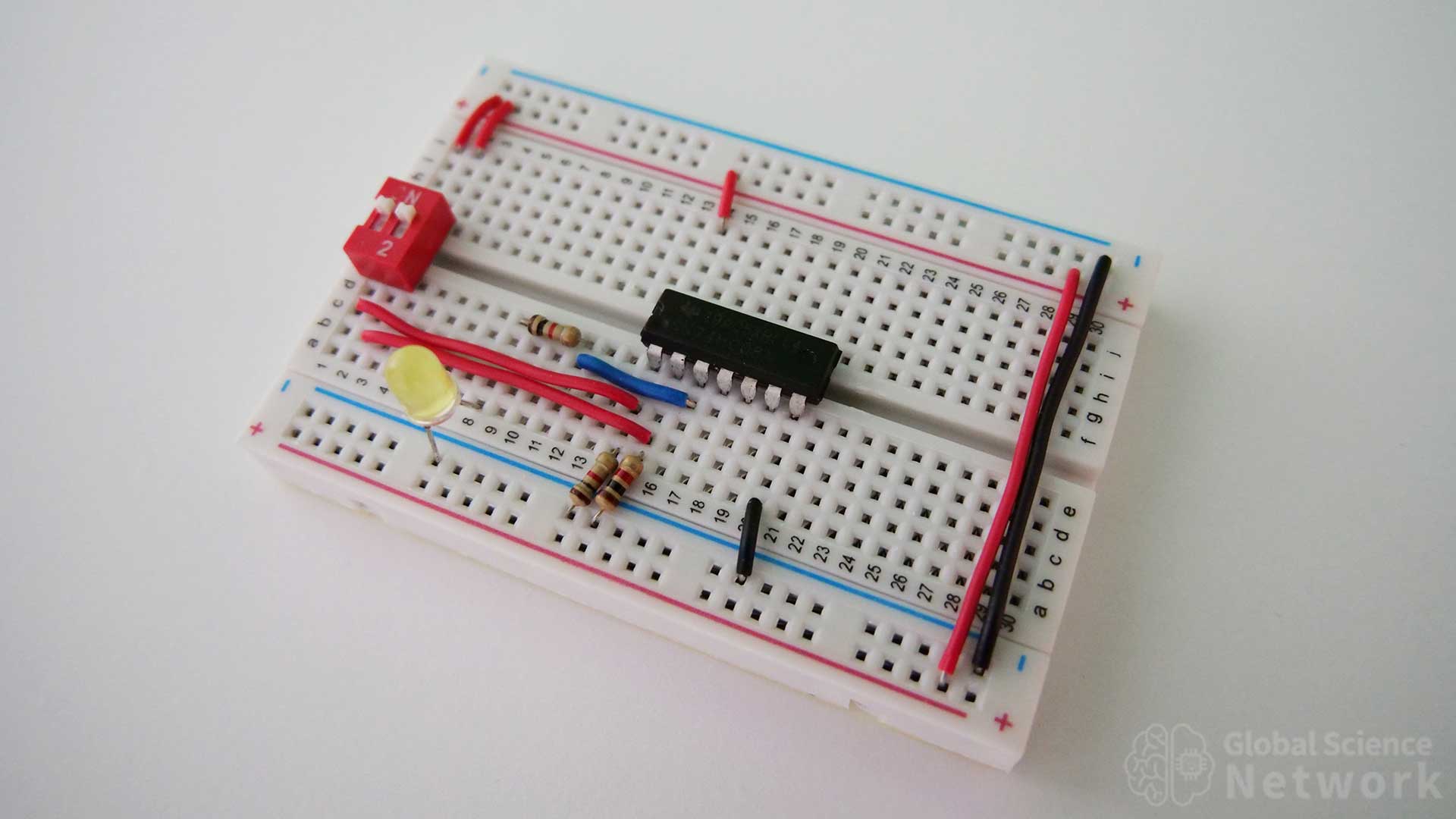
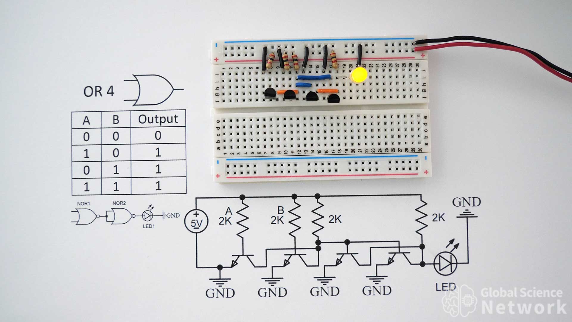
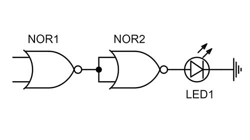
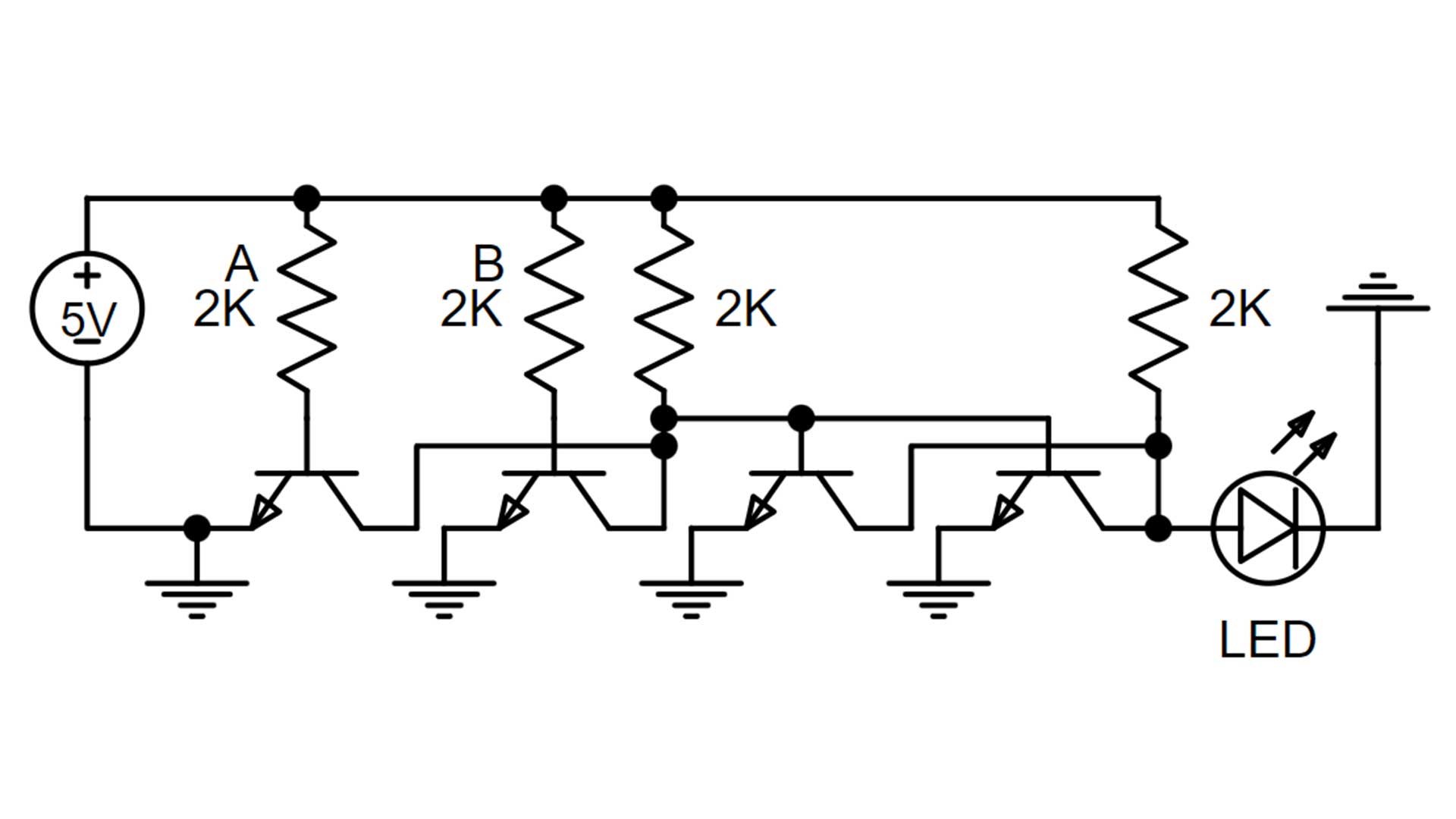
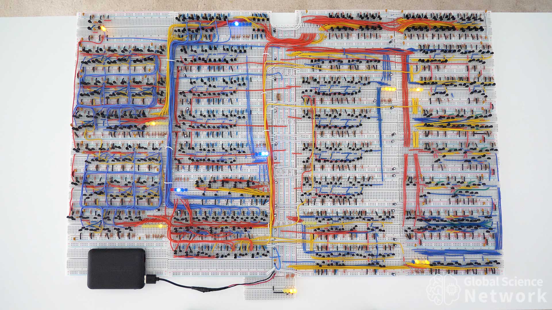
Breadboards are also designed to work with integrated circuits. An entire microprocessor can be placed on an integrated circuit so ICs drastically increase the potential of what can be done on a breadboard. Common integrated circuits to use on breadboards include logic gates, 555 timers, op-amps, shift registers, EPROM, FPGAs, gyroscopes, and microprocessors.
BreadBoard Tools
Wire Stripper
Buy from Amazon
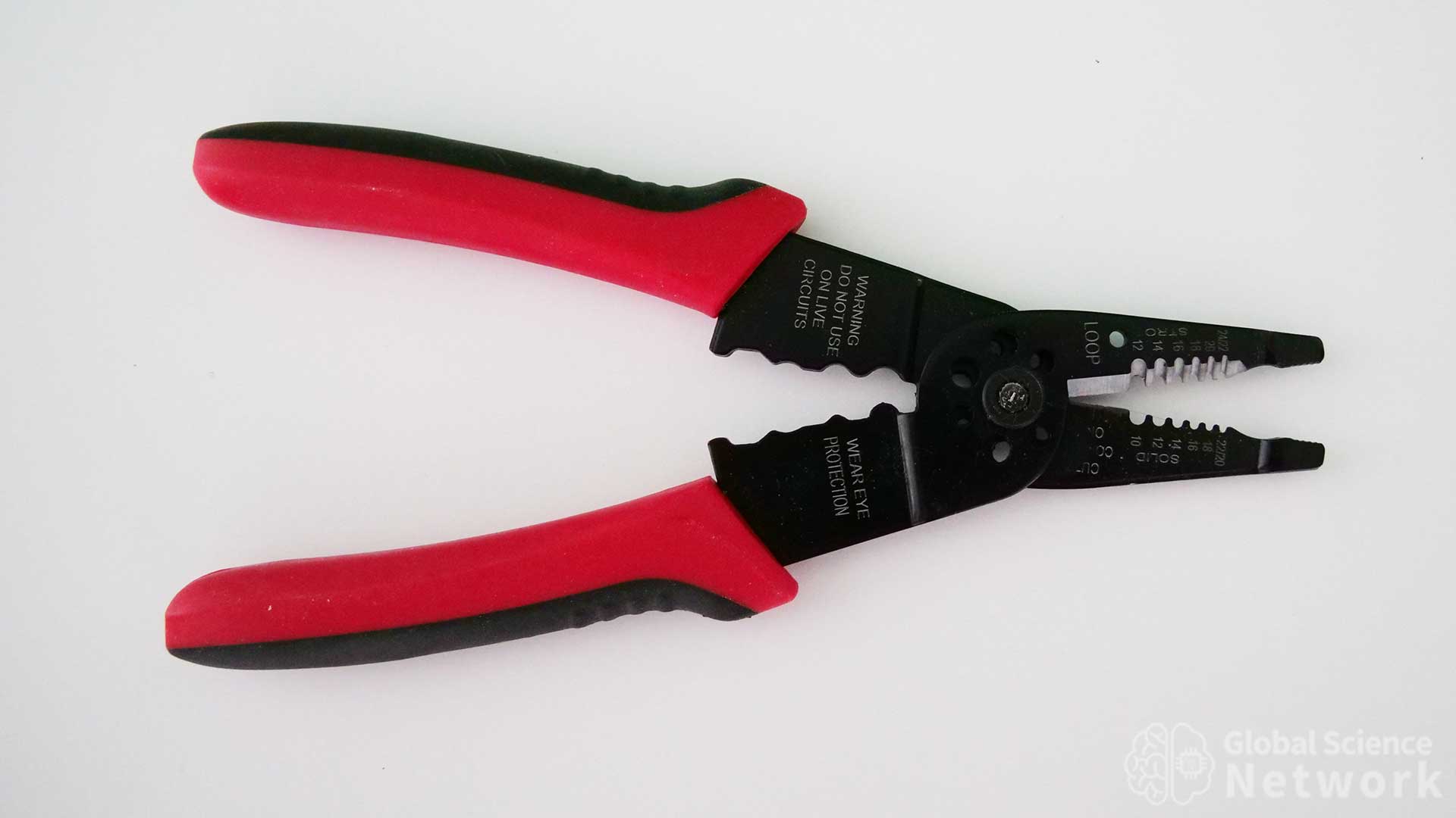
Wire strippers are needed to cut wires and remove the wire insulation on the end of the wire. Breadboard wires are 22 gauge so the stripper needs to have a slot to strip 22 gauge wire insulation. The wire stripper above can cut and strip wire from 10 gauge to 22 gauge. It also has a crimper to make crimp connections. When cutting breadboard wire to exact lengths some type of cutter and wire stripper is needed.
Wire Cutter
Buy from Amazon
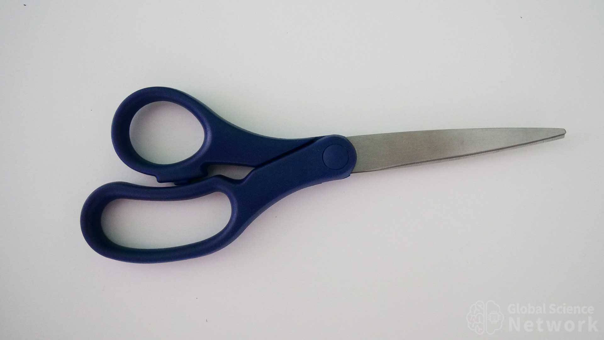
Scissors or a wire cutter make cutting wire much easier. The wire stripper tool does have a cutter but only on the back of the jaws. Having a tool with a cutter on the front jaws makes it easier to mark where the wire needs to be cut. Resistor wire is very thin and is easy to cut with scissors. I often cut multiple resistor wires down to the proper size with just one cut on each side. A small wire cutter is probably best but scissors do work if that is what is available.
Breadboard Power Supply
A breadboard can be powered by a variety of power supplies. Batteries used to be the most common way to power a breadboard. Two 1.5-volt batteries in series make a 3-volt power source. Three 1.5-volt batteries in series can be used to supply 4.5 volts. One 9-volt battery works with connector clips and power wires. There are also breadboard power supply modules that can provide 3.3V or 5 volts. The module can receive input power through a 2.1 mm jack plug or USB cable. The disadvantage of the breadboard module is that it takes up space on the breadboard. Power can also be sent from an Arduino, Raspberry Pi, or microcontroller to the breadboard.
USB Battery Pack
Buy from Amazon
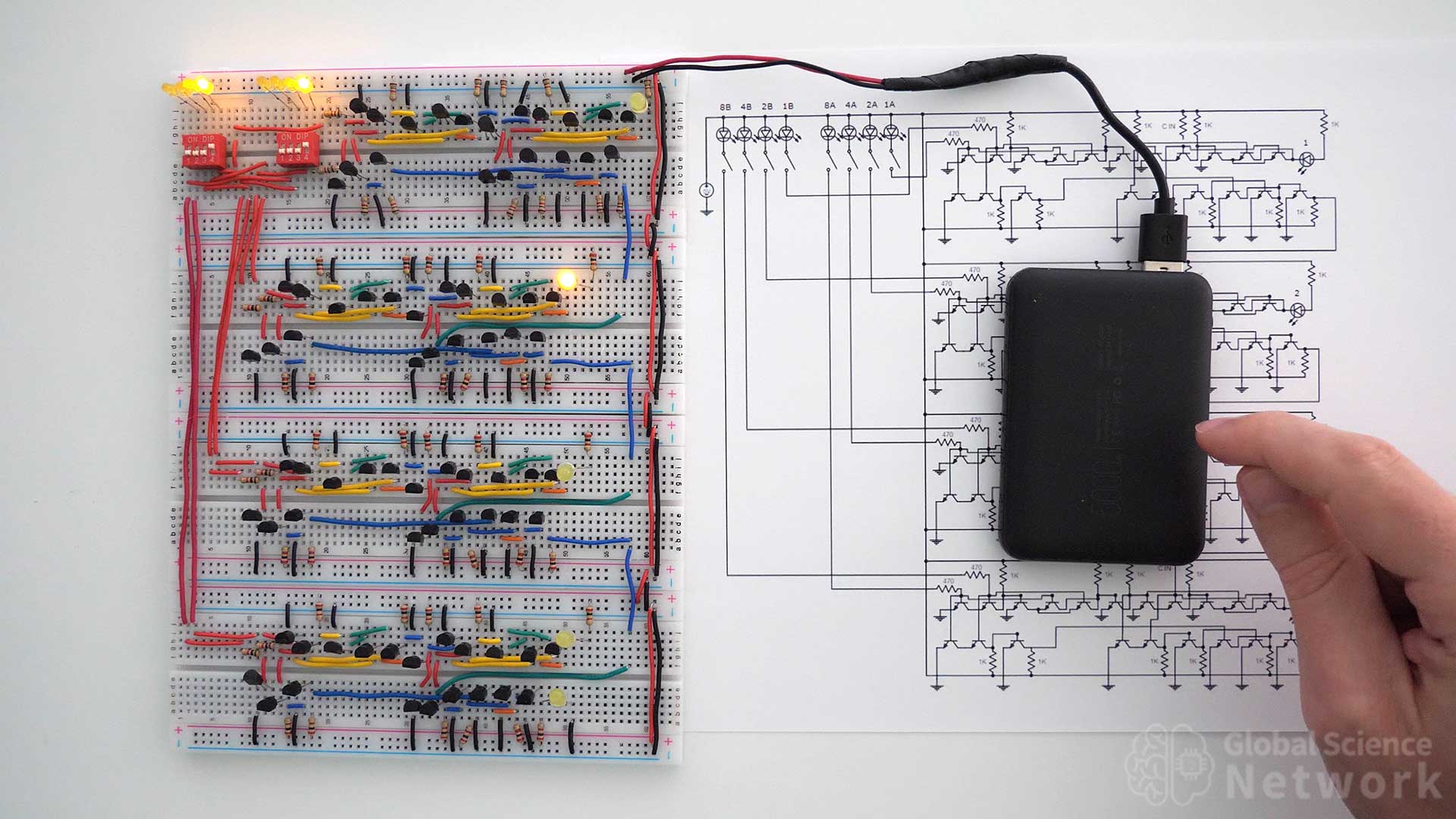
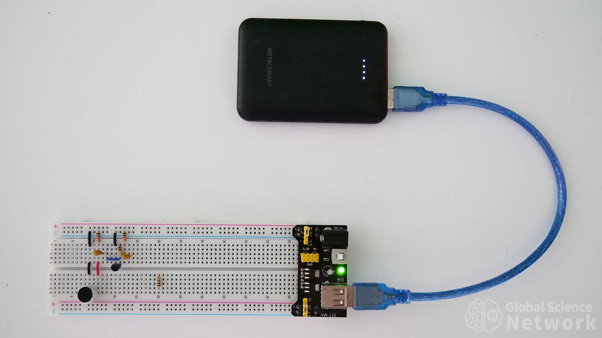
In the photo above I am providing power to a 4-bit calculator that is built on breadboards using a 5-volt battery pack. I modified a USB power cable so that it could go into the positive and negative terminals of the breadboard. This was done by splicing solid core 22 gauge wire from the stranded cable that was in the original power cable. The only downside to using this battery pack is it does have an auto shut-off feature if the output current is too low. It stops supply power after about 30 seconds when this is the case. Pushing the button on the battery pack will allow the current to flow for another 30 seconds. This is ok when testing circuits because you typically know within 30 seconds if the circuit is working properly. For larger circuits, it will not shut off as the current used is high enough to not shut the power off.
Cell Phone Charger and USB Cable
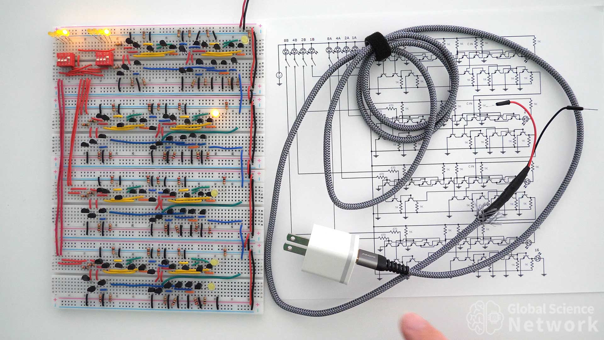
Using a 5-volt cell phone charger is becoming a popular way to power a breadboard. Most cell phone chargers and USB ports from computers provide a 5-volt power source. In the photo above I modified a 6-foot USB cable to have breadboard jumper cable ends. Now, most USB power supplies will work to power the breadboard at 5 volts.
External Circuit With USB Power Supply
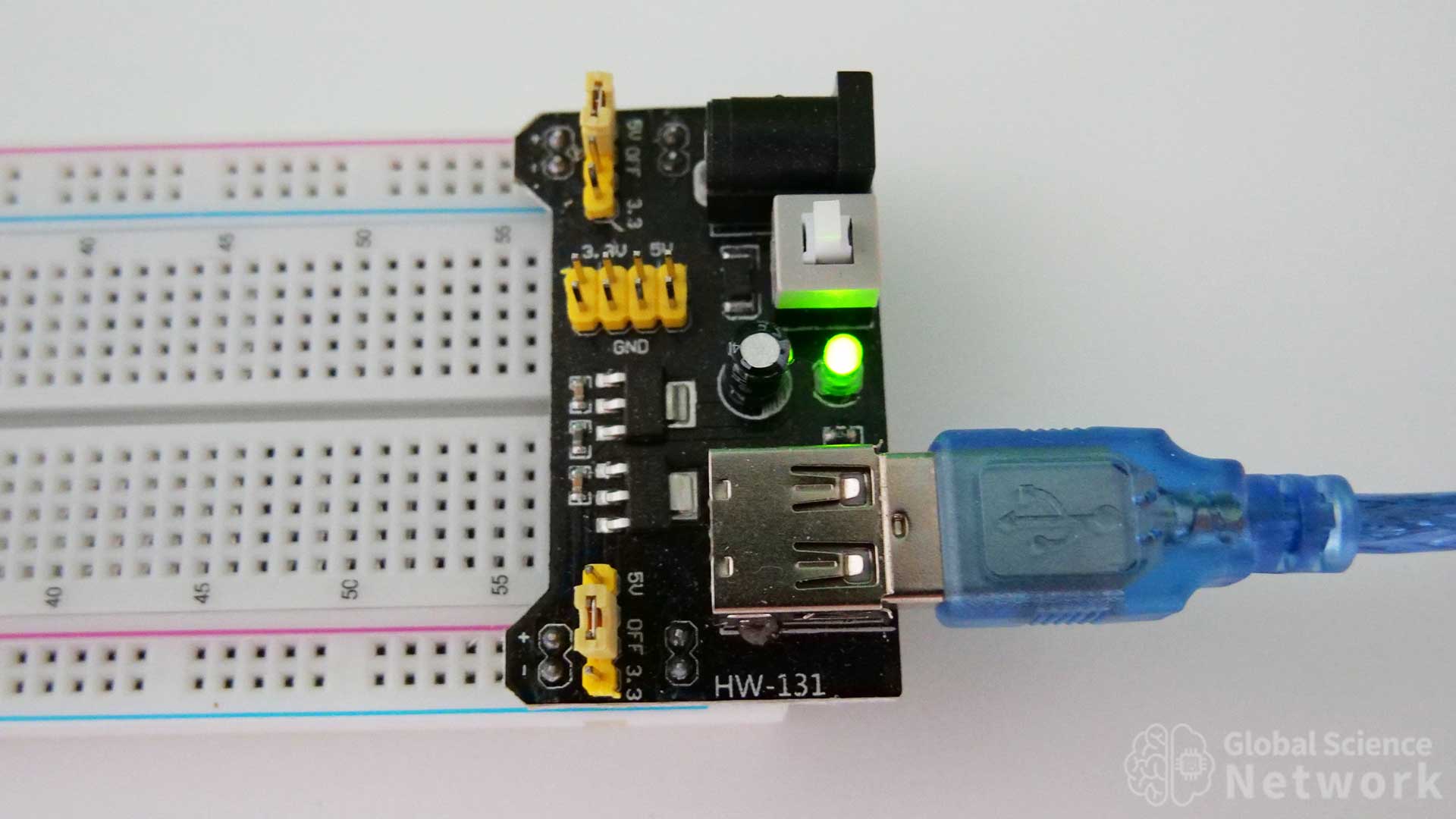
The photo above shows how to connect power to a breadboard power supply module using a USB cable. A 5-volt battery pack is supplying the power. The module receives power from the USB cable. Jumpers above each power rail can be moved so that 5 volts, zero volts, or 3.3 volts is supplied to the power rail. The top and bottom power rails can be set to different values. In the photo, the top power rail is set to 5 volts and the bottom power rail is set to zero volts. A green LED on the board indicated the power is being supplied to the board. There is a button that turns the power off to the board and the LED will shut off when power is not being supplied to the breadboard.
Power Supply Module
Buy from Amazon
The close-up view of the power supply modules shows all the features of the board. Input power can come from the jack plug or USB cable. Power going into the power jack needs to be between 6.5 and 9 volts. Power coming from the USB should be around 5 volts. The module is connected to the breadboard with 8 pins. Four pins on each side go into the power rails. This is an ok option to power a breadboard. I personally prefer when power is supplied over two wires. It makes it so there is more room on the breadboard and makes the breadboard less cluttered. When making demonstration videos it is also nice not having people wonder what is going on with the power supply. It is simpler to just show a red wire and a black wire going into the positive and negative slots in the breadboard.
Buy from Amazon
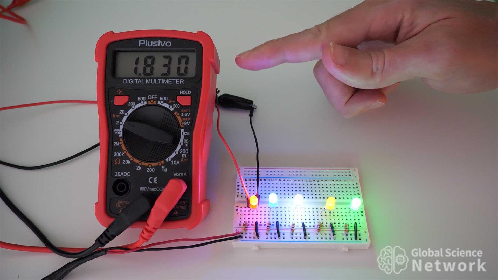
A multimeter provides a way of measuring the current in the circuit. It is also a way to measure the voltage levels within the circuit. I do use this multimeter to determine the current. For voltage levels though, I prefer to see the output on the oscilloscope as this provides transient information as well.
Buy from Amazon
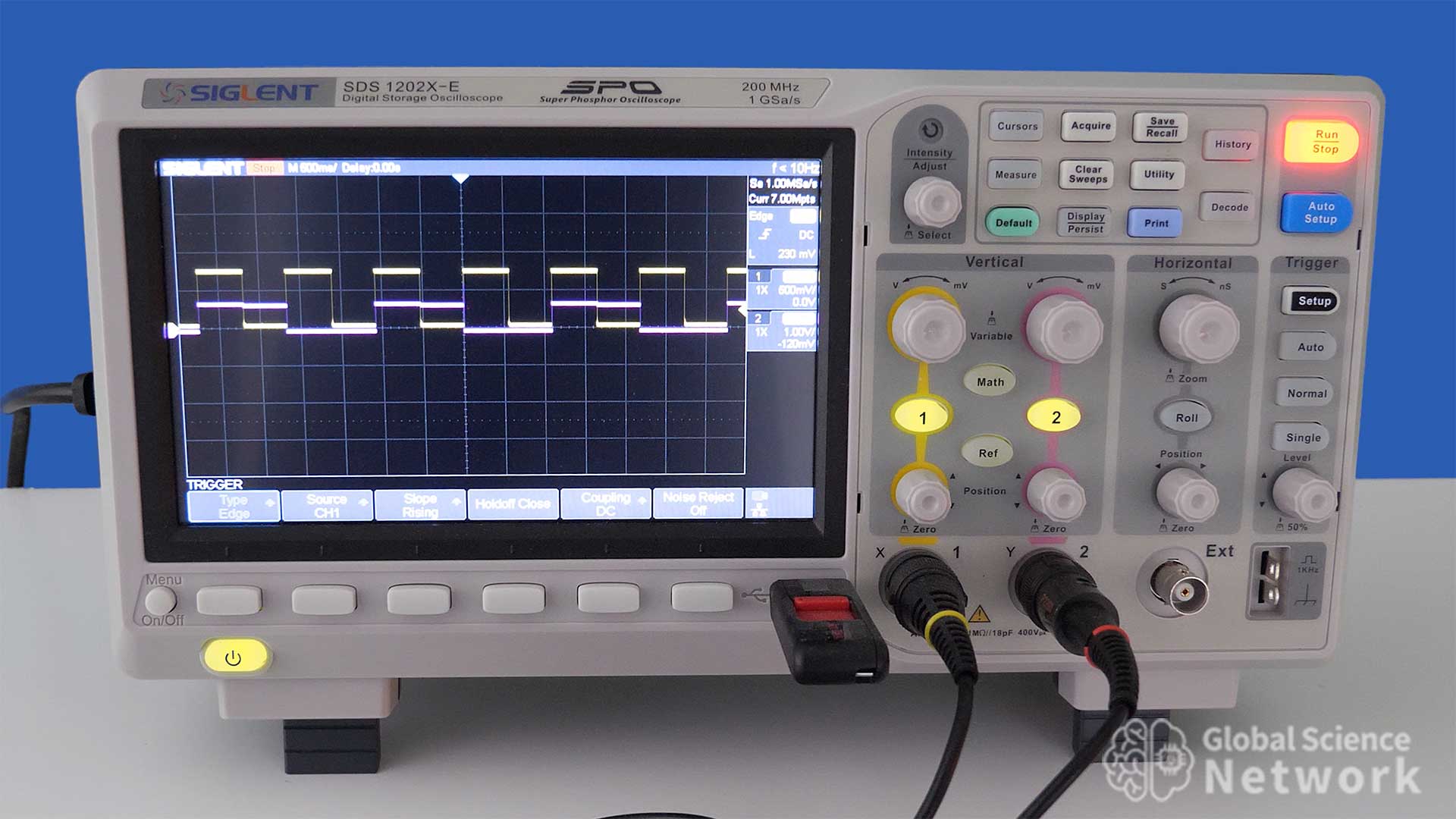
Having a digital oscilloscope is really handy when working with circuits. It is often difficult to know what is going on within the circuit without looking at the voltage values at different locations within the circuit. The oscilloscope not only shows the voltage values but shows the values over time so you can see transient conditions within the circuit.
Cody started the Global Science Network with the idea people should be focusing more time, energy, and resources on useful projects. He has a bachelor’s degree in aerospace engineering and a master’s degree in mechanical engineering. Cody has worked for the US federal government, a university, a large corporation, small businesses, and for himself. He has done human brain computer interface research and is currently working towards creating non-biological human consciousness.